- 您現(xiàn)在的位置:買賣IC網(wǎng) > PDF目錄385396 > HSP50214VC (INTERSIL CORP) Programmable Downconverter PDF資料下載
參數(shù)資料
| 型號: | HSP50214VC |
| 廠商: | INTERSIL CORP |
| 元件分類: | 通信及網(wǎng)絡 |
| 英文描述: | Programmable Downconverter |
| 中文描述: | SPECIALTY TELECOM CIRCUIT, PQFP120 |
| 封裝: | MQFP-120 |
| 文件頁數(shù): | 24/54頁 |
| 文件大?。?/td> | 395K |
| 代理商: | HSP50214VC |
第1頁第2頁第3頁第4頁第5頁第6頁第7頁第8頁第9頁第10頁第11頁第12頁第13頁第14頁第15頁第16頁第17頁第18頁第19頁第20頁第21頁第22頁第23頁當前第24頁第25頁第26頁第27頁第28頁第29頁第30頁第31頁第32頁第33頁第34頁第35頁第36頁第37頁第38頁第39頁第40頁第41頁第42頁第43頁第44頁第45頁第46頁第47頁第48頁第49頁第50頁第51頁第52頁第53頁第54頁

24
of instructions per second) effective due to symmetry. If the
CDMA filter (loaded into the programmable FIR section)
requires an impulse response with a span of 12 chips, the fil-
ter at 2x the chip-rate would need 24 taps. The 24 taps would
translate into 59MIPS = (1.2288MHz)(2)(24). To get the same
filtering at 8x the chip rate would require 944MIPS =
(1.2288MHz)(8)(96). Direct 8x filtering can not be accom-
plished with the programmable filter alone because 944MIPS
are much greater that the 60MIPs effective limit set by PROC-
CLK. It is necessary to decimate down to 2x the chip rate to
get a realistic number of filter taps. Both interpolation halfband
filters are used to obtain an 8x CDMA output. The MIPS for
the first halfband equals (2.4576MHz)(Number of Multiplies
for first halfband), and the second equal (4.9152MHz)(Num-
ber of Multiplies for second halfband). Combined halfband fil-
ters is equal to (1.2228MHz)(4)(48) = 236MIPS. Thus the
MIPS are 18 and 25 for the first and second halfbands respec-
tively, and 42 for both.
Timing NCO
The Timing NCO is very similar to the carrier NCO phase
accumulator section. It provides the NCO driven sample pulse
and associated phase information to the re-sampling filter pro-
cess described in the Resampler Filter section. The Timing
NCO does not include the SIN/COS section found in the Car-
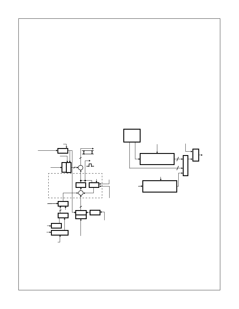
rier NCO. The top level block diagram is shown in Figure 26.
The programmable parameters for the Timing NCO include
an Enable External Timing NCO Sync (Control Word 11, bit
5), the serial word width, Number of Offset Frequency Bits
(Control Word 11 bits 3-4), an Enable Offset Frequency con-
trol (Control Word 11, bit 2), a Clear NCO Accumulator con-
trol (Control Word 11, bit 1), a Timing NCO Phase
Accumulator Load On Update control (Control Word 11, bit
0), the Timing NCO Center Frequency (Control Word 12), a
Timing Phase Offset (Control Word 13, bits 0-7), a Timing
Frequency Strobe (Control Word 14) and a Timing Phase
Strobe (Control Word 15). Refer to the Carrier Synthesizer
Mixer section for a detailed discussion of the serial interface
for the Timing NCO offset frequency word.
A timing error detector is provided for measuring the phase
difference between the timing NCO and a external clock input,
REFCLK. Timing Error is generated by comparing the values
of two programmable counters. One counter is clocked with
the Timing NCO carry out and the other is clocked by the
REFCLK. The 12-bit NCO Divide parameter is set in Control
Word 18, bits 16-27. The NCO Divide parameter is the pre-
load to the counter that is clocked by the Timing NCO carry
out. The 12-bit Reference Divide parameter is set in Control
Word 18, bits 0-11, and is the preload for the counter that is
clocked by the Reference clock. Figure 27 details the block
diagram of the timing error generation circuit. The 16 bits of
timing error are available both as a PDC serial output and as a
processor read parameter. See the Processor Read Section
for more details on accessing this value.
Figure 27A illustrates an application where the Timing Error
Generator is used to lock the receiver samples with a trans-
mit data rate. In this example, the receive samples are at
four times the transmit data rate. An external loop filter is
required, whose frequency error output is fed into the Timing
NCO. This allows the loop to track out the long term drift
between the receive sample rate and the transmit data clock.
SHIFT REG
SYNC
SOF
SOFSYNC
TIMING NCO CENTER
FREQUENCY
TIMING NCO
PHASE OFFSET
32
32
8
MUX
0
MUX
0
CLEAR
PHASE
ACC
PHASE
ACCUMULATOR
SCF
SOF
ENABLE SOF
REG
REG
+
Controlled via microprocessor interface.
5
TIMING PHASE STROBE
TIMING FREQ
STROBE
NUMBER OF SOF BITS
+
R
TIMING NCO
PH ACC
LOAD ON
UPDATE
R
REG
SYNC
SYNCIN2
EN EXT TIMING NCO SYNC
SYNC
CARRY OUT = RUN
FILTER STROBE
FILTER PHASE
SELECT
FIGURE 26. TIMING NCO BLOCK DIAGRAM
REG
Controlled via microprocessor interface.
FIGURE 27. TIMING ERROR GENERATION
PROGRAMMABLE
DIVIDER
PROGRAMMABLE
DIVIDER
REFERENCE
DIVIDE
TE(15:0)
C
REFCLK
R
+
P
NCO DIVIDE
(NCO DIVIDE)/2
-
12
4
EN
TIMING
NCO
ACC
HSP50214
相關PDF資料 |
PDF描述 |
|---|---|
| HSP50214VI | Programmable Downconverter |
| HSP50214 | Programmable Downconverter |
| HSP50215VC | Digital UpConverter |
| HSP50215VI | Digital UpConverter |
| HSP50215EVAL | DSP Modulator Evaluation Board |
相關代理商/技術參數(shù) |
參數(shù)描述 |
|---|---|
| HSP50214VI | 制造商:Rochester Electronics LLC 功能描述:- Bulk |
| HSP50215 | 制造商:INTERSIL 制造商全稱:Intersil Corporation 功能描述:DSP Modulator Evaluation Board |
| HSP50215EVAL | 制造商:INTERSIL 制造商全稱:Intersil Corporation 功能描述:DSP Modulator Evaluation Board |
| HSP50215VC | 制造商:INTERSIL 制造商全稱:Intersil Corporation 功能描述:Digital UpConverter |
| HSP50215VI | 制造商:INTERSIL 制造商全稱:Intersil Corporation 功能描述:Digital UpConverter |
發(fā)布緊急采購,3分鐘左右您將得到回復。