- 您現在的位置:買賣IC網 > PDF目錄4561 > DS3164N (Maxim Integrated Products)IC QUAD ATM/PACKET PHY 400-PBGA PDF資料下載
參數資料
| 型號: | DS3164N |
| 廠商: | Maxim Integrated Products |
| 文件頁數: | 304/384頁 |
| 文件大小: | 0K |
| 描述: | IC QUAD ATM/PACKET PHY 400-PBGA |
| 產品培訓模塊: | Lead (SnPb) Finish for COTS Obsolescence Mitigation Program |
| 標準包裝: | 1 |
| 類型: | PHY 收發(fā)器 |
| 應用: | 測試設備 |
| 安裝類型: | 表面貼裝 |
| 封裝/外殼: | 400-BBGA |
| 供應商設備封裝: | 400-PBGA(27x27) |
| 包裝: | 托盤 |
第1頁第2頁第3頁第4頁第5頁第6頁第7頁第8頁第9頁第10頁第11頁第12頁第13頁第14頁第15頁第16頁第17頁第18頁第19頁第20頁第21頁第22頁第23頁第24頁第25頁第26頁第27頁第28頁第29頁第30頁第31頁第32頁第33頁第34頁第35頁第36頁第37頁第38頁第39頁第40頁第41頁第42頁第43頁第44頁第45頁第46頁第47頁第48頁第49頁第50頁第51頁第52頁第53頁第54頁第55頁第56頁第57頁第58頁第59頁第60頁第61頁第62頁第63頁第64頁第65頁第66頁第67頁第68頁第69頁第70頁第71頁第72頁第73頁第74頁第75頁第76頁第77頁第78頁第79頁第80頁第81頁第82頁第83頁第84頁第85頁第86頁第87頁第88頁第89頁第90頁第91頁第92頁第93頁第94頁第95頁第96頁第97頁第98頁第99頁第100頁第101頁第102頁第103頁第104頁第105頁第106頁第107頁第108頁第109頁第110頁第111頁第112頁第113頁第114頁第115頁第116頁第117頁第118頁第119頁第120頁第121頁第122頁第123頁第124頁第125頁第126頁第127頁第128頁第129頁第130頁第131頁第132頁第133頁第134頁第135頁第136頁第137頁第138頁第139頁第140頁第141頁第142頁第143頁第144頁第145頁第146頁第147頁第148頁第149頁第150頁第151頁第152頁第153頁第154頁第155頁第156頁第157頁第158頁第159頁第160頁第161頁第162頁第163頁第164頁第165頁第166頁第167頁第168頁第169頁第170頁第171頁第172頁第173頁第174頁第175頁第176頁第177頁第178頁第179頁第180頁第181頁第182頁第183頁第184頁第185頁第186頁第187頁第188頁第189頁第190頁第191頁第192頁第193頁第194頁第195頁第196頁第197頁第198頁第199頁第200頁第201頁第202頁第203頁第204頁第205頁第206頁第207頁第208頁第209頁第210頁第211頁第212頁第213頁第214頁第215頁第216頁第217頁第218頁第219頁第220頁第221頁第222頁第223頁第224頁第225頁第226頁第227頁第228頁第229頁第230頁第231頁第232頁第233頁第234頁第235頁第236頁第237頁第238頁第239頁第240頁第241頁第242頁第243頁第244頁第245頁第246頁第247頁第248頁第249頁第250頁第251頁第252頁第253頁第254頁第255頁第256頁第257頁第258頁第259頁第260頁第261頁第262頁第263頁第264頁第265頁第266頁第267頁第268頁第269頁第270頁第271頁第272頁第273頁第274頁第275頁第276頁第277頁第278頁第279頁第280頁第281頁第282頁第283頁第284頁第285頁第286頁第287頁第288頁第289頁第290頁第291頁第292頁第293頁第294頁第295頁第296頁第297頁第298頁第299頁第300頁第301頁第302頁第303頁當前第304頁第305頁第306頁第307頁第308頁第309頁第310頁第311頁第312頁第313頁第314頁第315頁第316頁第317頁第318頁第319頁第320頁第321頁第322頁第323頁第324頁第325頁第326頁第327頁第328頁第329頁第330頁第331頁第332頁第333頁第334頁第335頁第336頁第337頁第338頁第339頁第340頁第341頁第342頁第343頁第344頁第345頁第346頁第347頁第348頁第349頁第350頁第351頁第352頁第353頁第354頁第355頁第356頁第357頁第358頁第359頁第360頁第361頁第362頁第363頁第364頁第365頁第366頁第367頁第368頁第369頁第370頁第371頁第372頁第373頁第374頁第375頁第376頁第377頁第378頁第379頁第380頁第381頁第382頁第383頁第384頁
DS3161/DS3162/DS3163/DS3164
17 DC ELECTRICAL CHARACTERISTICS
ABSOLUTE MAXIMUM RATINGS
Voltage Range on Any Input, Bidirectional or Open Drain
Output Lead Range with Respect to VSS.…………………………………………………………………...-0.3V to +5.5V
Supply Voltage (VDD) Range with Respect to VSS…………………………………………………………..-0.3V to +3.63V
Ambient Operating Temperature Range……………………………………………………………………..-40
°C to +85°C
Junction Operating Temperature Range……………………………………………………………………-40
°C to +125°C
Storage Temperature Range………………………………………………………………………………...-55°C to +125°C
Soldering Temperature Range..……………………………………………….See IPC/JEDEC J-STD-020 Specification.
These are stress ratings only and functional operation of the device at these or any other conditions beyond those indicated in the operation
sections of this specification is not implied. Exposure to absolute maximum rating conditions for extended periods of time can affect device
reliability. Ambient Operating Temperature Range is assuming the device is mounted on a JEDEC standard test board in a convection cooled
JEDEC test enclosure.
Note: The typical values listed below are not production tested.
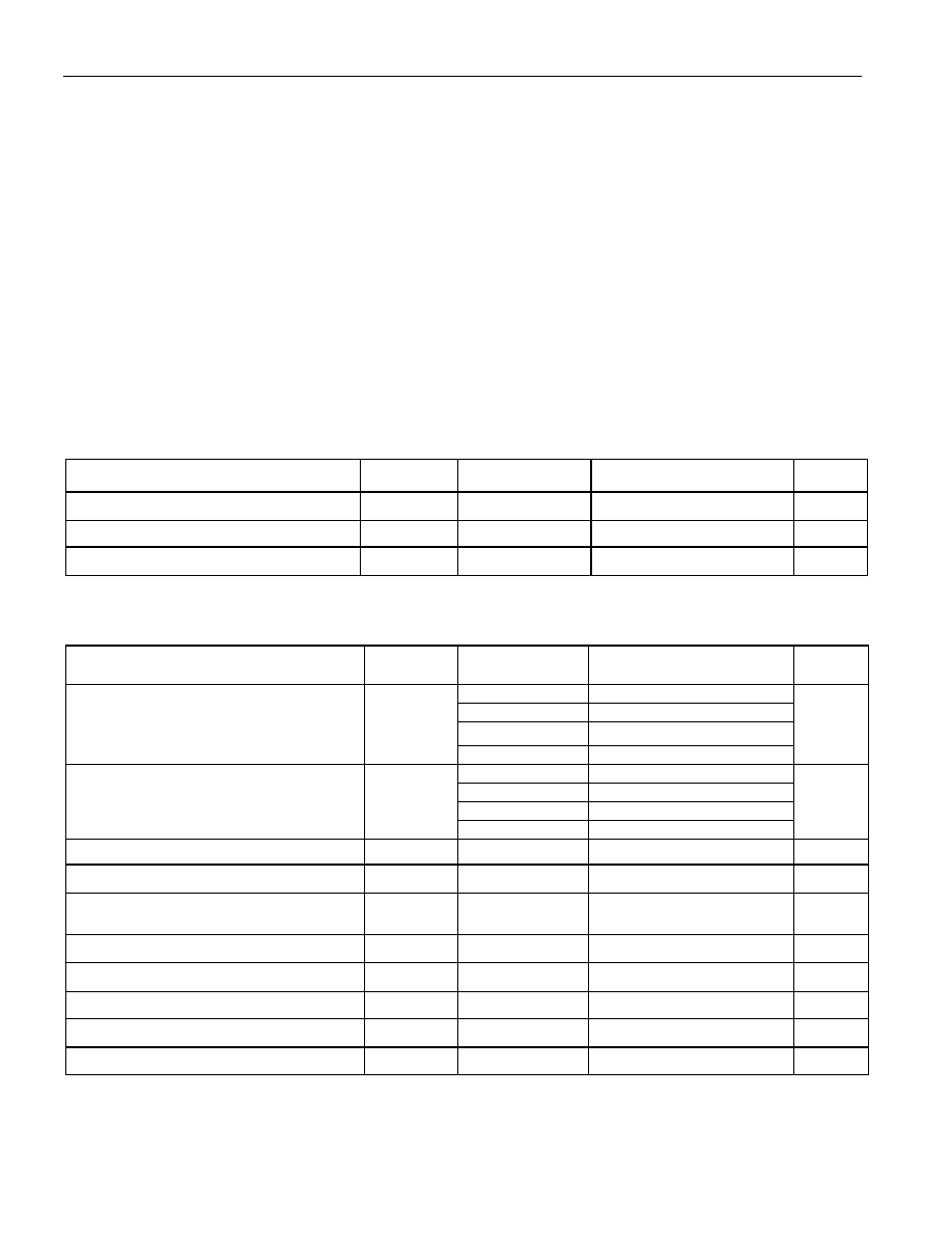
Table 17-1. Recommended DC Operating Conditions
(VDD = 3.3V ±5%, Tj = -40°C to +85°C.)
PARAMETER
SYMBOL
CONDITIONS
MIN
TYP
MAX
UNITS
Logic 1
VIH
2.0
5.5
V
Logic 0
VIL
-0.3
+0.8
V
Supply (VDD) ±5%
VDD
3.135
3.300
3.465
V
Table 17-2. DC Electrical Characteristics
(Tj = -40°C to +85°C)
PARAMETER
SYMBOL
CONDITIONS
MIN
TYP
MAX
UNITS
DS3164
468
DS3163
381
DS3162
300
Supply Current (VDD = 3.465V)
(Notes 1, 2)
IDD
DS3161
218
mA
DS3164
70
105
DS3163
72
DS3162
46
Power-Down Current (All DISABLE Bits
Set) (Note 2)
IDDD
DS3161
20
mA
Lead Capacitance
CIO
7
pF
Input Leakage
IIL
-10
+10
A
Input Leakage (Inputs Pins with Internal
Pullup Resistors)
IILP
-350
+10
A
Output Leakage (when High Impedance)
ILO
-10
+10
A
Output Voltage (IOH = -4.0mA)
VOH
4mA outputs
2.4
V
Output Voltage (IOL = +4.0mA)
VOL
4mA outputs
0.4
V
Output Voltage (IOH = -6.0mA)
VOH
6mA outputs
2.4
V
Output Voltage (IOL = +6.0mA)
VOL
6mA outputs
0.4
V
Note 1:
Mode: STS-1 data rate, transmitting all ones, all clocks = 52MHz, digital outputs without load.
Note 2:
All outputs loaded with rated capacitance; all inputs between VDD and VSS; inputs with pullups connected to VDD.
相關PDF資料 |
PDF描述 |
|---|---|
| AMC22DRYN-S93 | CONN EDGECARD 44POS DIP .100 SLD |
| AMC22DRYH-S93 | CONN EDGECARD 44POS DIP .100 SLD |
| 24LC00-I/SN | IC EEPROM 128BIT 400KHZ 8SOIC |
| 24AA08T-I/MNY | IC EEPROM 8KBIT 400KHZ 8TDFN |
| HMC35DRYI-S13 | CONN EDGECARD 70POS .100 EXTEND |
相關代理商/技術參數 |
參數描述 |
|---|---|
| DS3166 | 制造商:Maxim Integrated Products 功能描述:6 PORT ATM/PHY 676-TEPBGA - Trays |
| DS3166N | 制造商:Maxim Integrated Products 功能描述:6 PORT ATM/PHY 676-TEPBGA IND - Trays |
| DS3168 | 制造商:Maxim Integrated Products 功能描述:8 PORT ATM/PHY 676-TEBGA - Trays |
| DS3168N | 制造商:Maxim Integrated Products 功能描述:8 PORT ATM/PHY 676-TEPBGA IND - Trays |
| DS316CC-F8 | 制造商:Enhance Technology 功能描述:ULTRASTOR DS SPARE PART: ONE (1) 6G SAS JBOD CONTROLLER KIT - Bulk |
發(fā)布緊急采購,3分鐘左右您將得到回復。