- 您現(xiàn)在的位置:買(mǎi)賣(mài)IC網(wǎng) > PDF目錄36339 > 935268386557 (NXP SEMICONDUCTORS) SPECIALTY CONSUMER CIRCUIT, PBGA292 PDF資料下載
參數(shù)資料
| 型號(hào): | 935268386557 |
| 廠商: | NXP SEMICONDUCTORS |
| 元件分類(lèi): | 消費(fèi)家電 |
| 英文描述: | SPECIALTY CONSUMER CIRCUIT, PBGA292 |
| 封裝: | PLASTIC, SOT-553-1, BGA-292 |
| 文件頁(yè)數(shù): | 51/532頁(yè) |
| 文件大小: | 1895K |
| 代理商: | 935268386557 |
第1頁(yè)第2頁(yè)第3頁(yè)第4頁(yè)第5頁(yè)第6頁(yè)第7頁(yè)第8頁(yè)第9頁(yè)第10頁(yè)第11頁(yè)第12頁(yè)第13頁(yè)第14頁(yè)第15頁(yè)第16頁(yè)第17頁(yè)第18頁(yè)第19頁(yè)第20頁(yè)第21頁(yè)第22頁(yè)第23頁(yè)第24頁(yè)第25頁(yè)第26頁(yè)第27頁(yè)第28頁(yè)第29頁(yè)第30頁(yè)第31頁(yè)第32頁(yè)第33頁(yè)第34頁(yè)第35頁(yè)第36頁(yè)第37頁(yè)第38頁(yè)第39頁(yè)第40頁(yè)第41頁(yè)第42頁(yè)第43頁(yè)第44頁(yè)第45頁(yè)第46頁(yè)第47頁(yè)第48頁(yè)第49頁(yè)第50頁(yè)當(dāng)前第51頁(yè)第52頁(yè)第53頁(yè)第54頁(yè)第55頁(yè)第56頁(yè)第57頁(yè)第58頁(yè)第59頁(yè)第60頁(yè)第61頁(yè)第62頁(yè)第63頁(yè)第64頁(yè)第65頁(yè)第66頁(yè)第67頁(yè)第68頁(yè)第69頁(yè)第70頁(yè)第71頁(yè)第72頁(yè)第73頁(yè)第74頁(yè)第75頁(yè)第76頁(yè)第77頁(yè)第78頁(yè)第79頁(yè)第80頁(yè)第81頁(yè)第82頁(yè)第83頁(yè)第84頁(yè)第85頁(yè)第86頁(yè)第87頁(yè)第88頁(yè)第89頁(yè)第90頁(yè)第91頁(yè)第92頁(yè)第93頁(yè)第94頁(yè)第95頁(yè)第96頁(yè)第97頁(yè)第98頁(yè)第99頁(yè)第100頁(yè)第101頁(yè)第102頁(yè)第103頁(yè)第104頁(yè)第105頁(yè)第106頁(yè)第107頁(yè)第108頁(yè)第109頁(yè)第110頁(yè)第111頁(yè)第112頁(yè)第113頁(yè)第114頁(yè)第115頁(yè)第116頁(yè)第117頁(yè)第118頁(yè)第119頁(yè)第120頁(yè)第121頁(yè)第122頁(yè)第123頁(yè)第124頁(yè)第125頁(yè)第126頁(yè)第127頁(yè)第128頁(yè)第129頁(yè)第130頁(yè)第131頁(yè)第132頁(yè)第133頁(yè)第134頁(yè)第135頁(yè)第136頁(yè)第137頁(yè)第138頁(yè)第139頁(yè)第140頁(yè)第141頁(yè)第142頁(yè)第143頁(yè)第144頁(yè)第145頁(yè)第146頁(yè)第147頁(yè)第148頁(yè)第149頁(yè)第150頁(yè)第151頁(yè)第152頁(yè)第153頁(yè)第154頁(yè)第155頁(yè)第156頁(yè)第157頁(yè)第158頁(yè)第159頁(yè)第160頁(yè)第161頁(yè)第162頁(yè)第163頁(yè)第164頁(yè)第165頁(yè)第166頁(yè)第167頁(yè)第168頁(yè)第169頁(yè)第170頁(yè)第171頁(yè)第172頁(yè)第173頁(yè)第174頁(yè)第175頁(yè)第176頁(yè)第177頁(yè)第178頁(yè)第179頁(yè)第180頁(yè)第181頁(yè)第182頁(yè)第183頁(yè)第184頁(yè)第185頁(yè)第186頁(yè)第187頁(yè)第188頁(yè)第189頁(yè)第190頁(yè)第191頁(yè)第192頁(yè)第193頁(yè)第194頁(yè)第195頁(yè)第196頁(yè)第197頁(yè)第198頁(yè)第199頁(yè)第200頁(yè)第201頁(yè)第202頁(yè)第203頁(yè)第204頁(yè)第205頁(yè)第206頁(yè)第207頁(yè)第208頁(yè)第209頁(yè)第210頁(yè)第211頁(yè)第212頁(yè)第213頁(yè)第214頁(yè)第215頁(yè)第216頁(yè)第217頁(yè)第218頁(yè)第219頁(yè)第220頁(yè)第221頁(yè)第222頁(yè)第223頁(yè)第224頁(yè)第225頁(yè)第226頁(yè)第227頁(yè)第228頁(yè)第229頁(yè)第230頁(yè)第231頁(yè)第232頁(yè)第233頁(yè)第234頁(yè)第235頁(yè)第236頁(yè)第237頁(yè)第238頁(yè)第239頁(yè)第240頁(yè)第241頁(yè)第242頁(yè)第243頁(yè)第244頁(yè)第245頁(yè)第246頁(yè)第247頁(yè)第248頁(yè)第249頁(yè)第250頁(yè)第251頁(yè)第252頁(yè)第253頁(yè)第254頁(yè)第255頁(yè)第256頁(yè)第257頁(yè)第258頁(yè)第259頁(yè)第260頁(yè)第261頁(yè)第262頁(yè)第263頁(yè)第264頁(yè)第265頁(yè)第266頁(yè)第267頁(yè)第268頁(yè)第269頁(yè)第270頁(yè)第271頁(yè)第272頁(yè)第273頁(yè)第274頁(yè)第275頁(yè)第276頁(yè)第277頁(yè)第278頁(yè)第279頁(yè)第280頁(yè)第281頁(yè)第282頁(yè)第283頁(yè)第284頁(yè)第285頁(yè)第286頁(yè)第287頁(yè)第288頁(yè)第289頁(yè)第290頁(yè)第291頁(yè)第292頁(yè)第293頁(yè)第294頁(yè)第295頁(yè)第296頁(yè)第297頁(yè)第298頁(yè)第299頁(yè)第300頁(yè)第301頁(yè)第302頁(yè)第303頁(yè)第304頁(yè)第305頁(yè)第306頁(yè)第307頁(yè)第308頁(yè)第309頁(yè)第310頁(yè)第311頁(yè)第312頁(yè)第313頁(yè)第314頁(yè)第315頁(yè)第316頁(yè)第317頁(yè)第318頁(yè)第319頁(yè)第320頁(yè)第321頁(yè)第322頁(yè)第323頁(yè)第324頁(yè)第325頁(yè)第326頁(yè)第327頁(yè)第328頁(yè)第329頁(yè)第330頁(yè)第331頁(yè)第332頁(yè)第333頁(yè)第334頁(yè)第335頁(yè)第336頁(yè)第337頁(yè)第338頁(yè)第339頁(yè)第340頁(yè)第341頁(yè)第342頁(yè)第343頁(yè)第344頁(yè)第345頁(yè)第346頁(yè)第347頁(yè)第348頁(yè)第349頁(yè)第350頁(yè)第351頁(yè)第352頁(yè)第353頁(yè)第354頁(yè)第355頁(yè)第356頁(yè)第357頁(yè)第358頁(yè)第359頁(yè)第360頁(yè)第361頁(yè)第362頁(yè)第363頁(yè)第364頁(yè)第365頁(yè)第366頁(yè)第367頁(yè)第368頁(yè)第369頁(yè)第370頁(yè)第371頁(yè)第372頁(yè)第373頁(yè)第374頁(yè)第375頁(yè)第376頁(yè)第377頁(yè)第378頁(yè)第379頁(yè)第380頁(yè)第381頁(yè)第382頁(yè)第383頁(yè)第384頁(yè)第385頁(yè)第386頁(yè)第387頁(yè)第388頁(yè)第389頁(yè)第390頁(yè)第391頁(yè)第392頁(yè)第393頁(yè)第394頁(yè)第395頁(yè)第396頁(yè)第397頁(yè)第398頁(yè)第399頁(yè)第400頁(yè)第401頁(yè)第402頁(yè)第403頁(yè)第404頁(yè)第405頁(yè)第406頁(yè)第407頁(yè)第408頁(yè)第409頁(yè)第410頁(yè)第411頁(yè)第412頁(yè)第413頁(yè)第414頁(yè)第415頁(yè)第416頁(yè)第417頁(yè)第418頁(yè)第419頁(yè)第420頁(yè)第421頁(yè)第422頁(yè)第423頁(yè)第424頁(yè)第425頁(yè)第426頁(yè)第427頁(yè)第428頁(yè)第429頁(yè)第430頁(yè)第431頁(yè)第432頁(yè)第433頁(yè)第434頁(yè)第435頁(yè)第436頁(yè)第437頁(yè)第438頁(yè)第439頁(yè)第440頁(yè)第441頁(yè)第442頁(yè)第443頁(yè)第444頁(yè)第445頁(yè)第446頁(yè)第447頁(yè)第448頁(yè)第449頁(yè)第450頁(yè)第451頁(yè)第452頁(yè)第453頁(yè)第454頁(yè)第455頁(yè)第456頁(yè)第457頁(yè)第458頁(yè)第459頁(yè)第460頁(yè)第461頁(yè)第462頁(yè)第463頁(yè)第464頁(yè)第465頁(yè)第466頁(yè)第467頁(yè)第468頁(yè)第469頁(yè)第470頁(yè)第471頁(yè)第472頁(yè)第473頁(yè)第474頁(yè)第475頁(yè)第476頁(yè)第477頁(yè)第478頁(yè)第479頁(yè)第480頁(yè)第481頁(yè)第482頁(yè)第483頁(yè)第484頁(yè)第485頁(yè)第486頁(yè)第487頁(yè)第488頁(yè)第489頁(yè)第490頁(yè)第491頁(yè)第492頁(yè)第493頁(yè)第494頁(yè)第495頁(yè)第496頁(yè)第497頁(yè)第498頁(yè)第499頁(yè)第500頁(yè)第501頁(yè)第502頁(yè)第503頁(yè)第504頁(yè)第505頁(yè)第506頁(yè)第507頁(yè)第508頁(yè)第509頁(yè)第510頁(yè)第511頁(yè)第512頁(yè)第513頁(yè)第514頁(yè)第515頁(yè)第516頁(yè)第517頁(yè)第518頁(yè)第519頁(yè)第520頁(yè)第521頁(yè)第522頁(yè)第523頁(yè)第524頁(yè)第525頁(yè)第526頁(yè)第527頁(yè)第528頁(yè)第529頁(yè)第530頁(yè)第531頁(yè)第532頁(yè)
TM1300 Data Book
Philips Semiconductors
9-6
PRODUCT SPECIFICATION
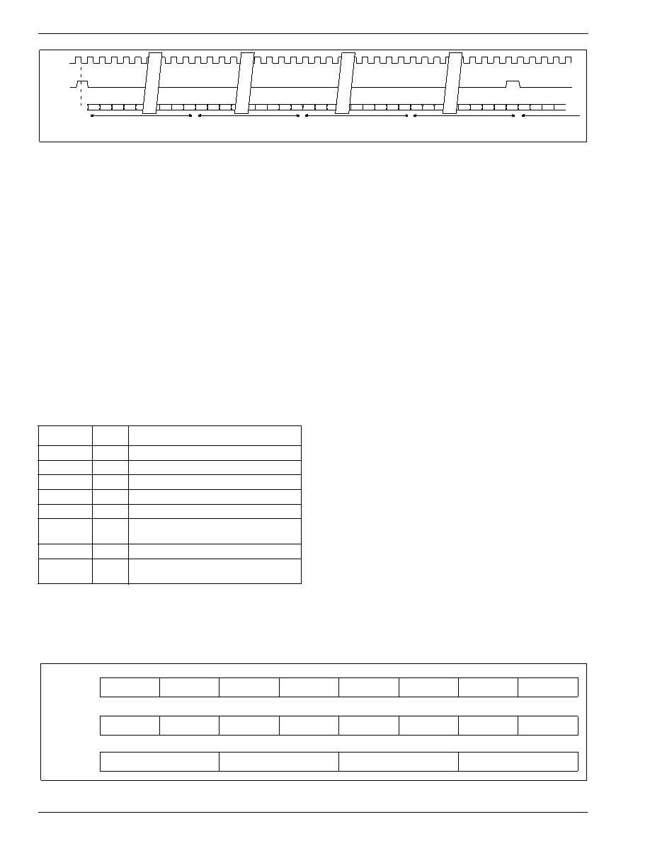
Figure 9-4 shows a 64-bit frame suitable for use with the
CS4218 codec. It is obtained by setting POLARITY=1,
LEFTPOS=0,
RIGHTPOS=32,
DATAMODE=0,
SS-
POS=0, CLOCK_EDGE=1, WS_PULSE=1, CC1_POS =
16, CC1_EN=1, CC2_POS=48, CC2_EN=1.
Note that frames are generated (externally or internally)
even when TRANS_ENABLE is de-asserted. Writes to
CC1
and
CC2
should
only
be
done
after
TRANS_ENABLE is asserted. The ‘first’ CC values will
then go out on the next frame. For a summary of codec
control fields see Table 9-8
9.9
MEMORY DATA FORMATS
The AO unit autonomously reads samples from memory
in 16 or 32 bit-per-sample memory formats, as shown in
Figure 9-5 for some example modes. Memory samples
are retrieved and used as described in Table 9-9. Suc-
cessive samples are always read from increasing mem-
ory
address
locations.
The
setting
of
the
LITTLE_ENDIAN bit in the AO_CTL register determines
the byte order of retrieved 16 or 32-bit samples. Refer to
Appendix C, “Endian-ness,”
for details on byte ordering con-
ventions.
AO hardware implements a double buffering scheme to
ensure that there are always samples available to trans-
mit, even if the DSPCPU is highly loaded and slow to re-
spond to interrupts. The DSPCPU software assigns 2
equal size buffers by writing a base address and size to
the MMIO control fields described in Figure 9-6. Refer to
Section 9.10, “Audio Out Operation,” for details on hard-
ware/software synchronization.
If SIGN_CONVERT is set to one, the MSB of the memo-
ry data is inverted, which is equivalent to translating from
offset binary representation to two’s complement. This
allows the use of an external two’s complement 16-bit D/
A converter to generate audio from 16-bit unsigned sam-
ples. This MSB inversion also applies to the ‘0’ values
transmitted to non-active output channels.
Note that the AO hardware does
not support A-law or
-
law eight-bit data formats. If such formats are desired,
the DSPCPU should be used to convert from A-law or
-
law data to 16-bit linear data.
Table 9-9. Operating modes and memory formats
NR_CHAN MODE
destination of successive samples
00
mono
SD1.left
00
stereo
SD1.left, SD1.right
01
mono
SD1.left, SD2.left
01
stereo
SD1.left, SD1.right, SD2.left, SD2.right
10
mono
SD1.left, SD2.left, SD3.left
10
stereo
SD1.left, SD1.right, SD2.left, SD2.right,
SD3.left, SD3.right
11
mono
SD1.left, SD2.left, SD3.left, SD4.left
11
stereo
SD1.left, SD1.right, SD2.left, SD2.right,
SD3.left, SD3.right, SD4.left, SD4.right.
Figure 9-4. Example codec frame layout for a Crystal Semi, CS4218.
1
63
62
48
47
32
31
3
2
1
0
left datan+1(16)
left channel datan(16)
right channel datan(16)
15
CC1(16)
16
lsb
CC2(16)
lsb
AO_SCK
AO_WS
AO_SDx
Figure 9-5. AO memory DMA formats.
adr
SD1.leftn
adr+2
SD1.rightn
adr+4
SD1.leftn+1
adr+6
SD1.rightn+1
adr+8
SD1.leftn+2
adr+10
SD1.rightn+2
adr+12
SD1.leftn+3
adr+14
SD1.rightn+3
16-bit, stereo,
NR_CHAN=00
32-bit, stereo,
NR_CHAN=00
SD1.leftn
adr
SD1.rightn
adr+4
SD1.leftn+1
adr+8
SD1.rightn+1
adr+12
adr
SD1.leftn
adr+2
SD1.rightn
adr+4
SD2.leftn
adr+6
SD2.rightn
adr+8
SD3.leftn
adr+10
SD3.rightn
adr+12
SD1.leftn+1
adr+14
SD1.rightn+1
16-bit, stereo,
NR_CHAN=10
相關(guān)PDF資料 |
PDF描述 |
|---|---|
| 935267050025 | SPECIALTY CONSUMER CIRCUIT, UUC |
| 935267053005 | SPECIALTY CONSUMER CIRCUIT, UUC |
| 935267052005 | SPECIALTY CONSUMER CIRCUIT, UUC |
| 935267395518 | COLOR SIGNAL DECODER, PBGA156 |
| 935267395551 | COLOR SIGNAL DECODER, PBGA156 |
相關(guān)代理商/技術(shù)參數(shù) |
參數(shù)描述 |
|---|---|
| 935268721125 | 制造商:NXP Semiconductors 功能描述:Buffer/Line Driver 1-CH Non-Inverting 3-ST CMOS 5-Pin TSSOP T/R |
| 935269304128 | 制造商:ST-Ericsson 功能描述:IC AUDIO CODEC W/TCH SCRN 48LQFP |
| 935269544557 | 制造商:NXP Semiconductors 功能描述:SUB ONLY TDA9587-2US1-V1.3 |
| 935269987557 | 制造商:NXP Semiconductors 功能描述:SUB ONLY TDA9587-1US1-V1.8 SUBBED TO 935269987557 |
| 935270713557 | 制造商:NXP Semiconductors 功能描述:SUB ONLY IC CHP |
發(fā)布緊急采購(gòu),3分鐘左右您將得到回復(fù)。