- 您現(xiàn)在的位置:買賣IC網(wǎng) > PDF目錄36339 > 935268386557 (NXP SEMICONDUCTORS) SPECIALTY CONSUMER CIRCUIT, PBGA292 PDF資料下載
參數(shù)資料
| 型號: | 935268386557 |
| 廠商: | NXP SEMICONDUCTORS |
| 元件分類: | 消費家電 |
| 英文描述: | SPECIALTY CONSUMER CIRCUIT, PBGA292 |
| 封裝: | PLASTIC, SOT-553-1, BGA-292 |
| 文件頁數(shù): | 487/532頁 |
| 文件大小: | 1895K |
| 代理商: | 935268386557 |
第1頁第2頁第3頁第4頁第5頁第6頁第7頁第8頁第9頁第10頁第11頁第12頁第13頁第14頁第15頁第16頁第17頁第18頁第19頁第20頁第21頁第22頁第23頁第24頁第25頁第26頁第27頁第28頁第29頁第30頁第31頁第32頁第33頁第34頁第35頁第36頁第37頁第38頁第39頁第40頁第41頁第42頁第43頁第44頁第45頁第46頁第47頁第48頁第49頁第50頁第51頁第52頁第53頁第54頁第55頁第56頁第57頁第58頁第59頁第60頁第61頁第62頁第63頁第64頁第65頁第66頁第67頁第68頁第69頁第70頁第71頁第72頁第73頁第74頁第75頁第76頁第77頁第78頁第79頁第80頁第81頁第82頁第83頁第84頁第85頁第86頁第87頁第88頁第89頁第90頁第91頁第92頁第93頁第94頁第95頁第96頁第97頁第98頁第99頁第100頁第101頁第102頁第103頁第104頁第105頁第106頁第107頁第108頁第109頁第110頁第111頁第112頁第113頁第114頁第115頁第116頁第117頁第118頁第119頁第120頁第121頁第122頁第123頁第124頁第125頁第126頁第127頁第128頁第129頁第130頁第131頁第132頁第133頁第134頁第135頁第136頁第137頁第138頁第139頁第140頁第141頁第142頁第143頁第144頁第145頁第146頁第147頁第148頁第149頁第150頁第151頁第152頁第153頁第154頁第155頁第156頁第157頁第158頁第159頁第160頁第161頁第162頁第163頁第164頁第165頁第166頁第167頁第168頁第169頁第170頁第171頁第172頁第173頁第174頁第175頁第176頁第177頁第178頁第179頁第180頁第181頁第182頁第183頁第184頁第185頁第186頁第187頁第188頁第189頁第190頁第191頁第192頁第193頁第194頁第195頁第196頁第197頁第198頁第199頁第200頁第201頁第202頁第203頁第204頁第205頁第206頁第207頁第208頁第209頁第210頁第211頁第212頁第213頁第214頁第215頁第216頁第217頁第218頁第219頁第220頁第221頁第222頁第223頁第224頁第225頁第226頁第227頁第228頁第229頁第230頁第231頁第232頁第233頁第234頁第235頁第236頁第237頁第238頁第239頁第240頁第241頁第242頁第243頁第244頁第245頁第246頁第247頁第248頁第249頁第250頁第251頁第252頁第253頁第254頁第255頁第256頁第257頁第258頁第259頁第260頁第261頁第262頁第263頁第264頁第265頁第266頁第267頁第268頁第269頁第270頁第271頁第272頁第273頁第274頁第275頁第276頁第277頁第278頁第279頁第280頁第281頁第282頁第283頁第284頁第285頁第286頁第287頁第288頁第289頁第290頁第291頁第292頁第293頁第294頁第295頁第296頁第297頁第298頁第299頁第300頁第301頁第302頁第303頁第304頁第305頁第306頁第307頁第308頁第309頁第310頁第311頁第312頁第313頁第314頁第315頁第316頁第317頁第318頁第319頁第320頁第321頁第322頁第323頁第324頁第325頁第326頁第327頁第328頁第329頁第330頁第331頁第332頁第333頁第334頁第335頁第336頁第337頁第338頁第339頁第340頁第341頁第342頁第343頁第344頁第345頁第346頁第347頁第348頁第349頁第350頁第351頁第352頁第353頁第354頁第355頁第356頁第357頁第358頁第359頁第360頁第361頁第362頁第363頁第364頁第365頁第366頁第367頁第368頁第369頁第370頁第371頁第372頁第373頁第374頁第375頁第376頁第377頁第378頁第379頁第380頁第381頁第382頁第383頁第384頁第385頁第386頁第387頁第388頁第389頁第390頁第391頁第392頁第393頁第394頁第395頁第396頁第397頁第398頁第399頁第400頁第401頁第402頁第403頁第404頁第405頁第406頁第407頁第408頁第409頁第410頁第411頁第412頁第413頁第414頁第415頁第416頁第417頁第418頁第419頁第420頁第421頁第422頁第423頁第424頁第425頁第426頁第427頁第428頁第429頁第430頁第431頁第432頁第433頁第434頁第435頁第436頁第437頁第438頁第439頁第440頁第441頁第442頁第443頁第444頁第445頁第446頁第447頁第448頁第449頁第450頁第451頁第452頁第453頁第454頁第455頁第456頁第457頁第458頁第459頁第460頁第461頁第462頁第463頁第464頁第465頁第466頁第467頁第468頁第469頁第470頁第471頁第472頁第473頁第474頁第475頁第476頁第477頁第478頁第479頁第480頁第481頁第482頁第483頁第484頁第485頁第486頁當前第487頁第488頁第489頁第490頁第491頁第492頁第493頁第494頁第495頁第496頁第497頁第498頁第499頁第500頁第501頁第502頁第503頁第504頁第505頁第506頁第507頁第508頁第509頁第510頁第511頁第512頁第513頁第514頁第515頁第516頁第517頁第518頁第519頁第520頁第521頁第522頁第523頁第524頁第525頁第526頁第527頁第528頁第529頁第530頁第531頁第532頁
TM1300 Data Book
Philips Semiconductors
3-8
PRODUCT SPECIFICATION
for PC-hosted TM1300 boards; its final location is deter-
mined by the boot EEPROM for standalone systems.
See Chapter 13, “System Boot” for more information.
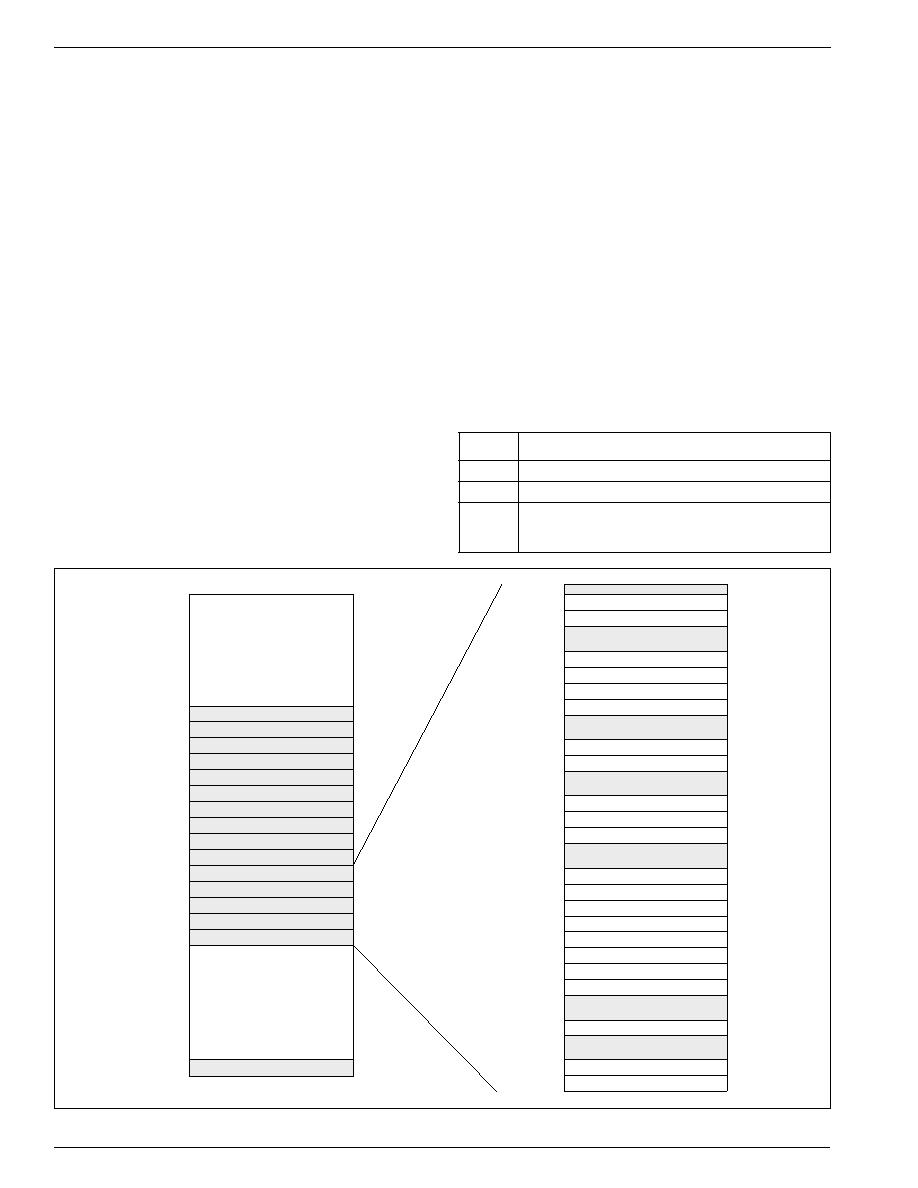
Figure 3-5 gives a detailed overview of the MMIO mem-
ory map (addresses used are offsets with respect to the
MMIO base). The operating system on TM1300 can
change MMIO_BASE by writing to the MMIO_BASE
MMIO location. User programs should not attempt this.
Refer to the TriMedia SDE Reference Manual for the
standard method to access the device registers from C
language device drivers.
Only 32-bit load and store operations are allowed to ac-
cess MMIO registers in the MMIO address aperture. The
results are undefined for other loads and stores. Reads
from non-existent MMIO registers return undefined val-
ues. Writes to nonexistent MMIO registers time out.
There are no side effects of accesses to nonexistent
MMIO registers. The state of the PCSW BSX bit has no
effect on the result of MMIO accesses.
The Icache tag and LRU bit access aperture give the
DSPCPU read-only access to the Icache status. Refer to
Section 5.4.8, “Reading Tags and Cache Status” for de-
tails.
The EXCVEC MMIO location is explained in Section
3.5.2, “EXC (Exceptions).” Section 3.5.3, “INT and NMI
(Maskable and Non-Maskable Interrupts),”
describes
the locations that deal with the setup and handling of in-
terrupts: ISETTING, IPENDING, ICLEAR, IMASK and
the interrupt vectors. The timer MMIO locations are de-
scribed in Section 3.8, “Timers.”
The instruction and
data breakpoint are described in Section 3.9, “Debug
Support.” The MMIO locations of each device are treat-
ed in the respective device chapters.
3.5
SPECIAL EVENT HANDLING
The TM1300 microprocessor responds to the special
events shown in Table 3-9, ordered by priority.
With the exception of RESET, which is enabled at all
times, the architecture of the DSPCPU allows special
event handling to begin only during an
interruptible jump
operation (ijmpt, ijmpf or ijmpi) that succeeds (i.e., is a
taken jump). EXC, NMI and INT handling can be initiated
during handling of an EXC or an INT, but
only during suc-
cessful interruptible jumps.
0x00 0000
Reserved
for
Future Use
Reserved
for
Future Use
0x10 3800
JTAG interface
0x10 3400
I2C interface
0x10 3000
PCI interface
0x10 2C00
SSI interface
0x10 2800
VLD coprocessor
0x10 2400
Image coprocessor
0x10 2000
Audio Out
0x10 1C00
Audio In
0x10 1800
Video Out
0x10 1400
Video In
0x10 1000
Debug support
0x10 0C00
Timers
0x10 0800
Vectored interrupt controller
0x10 0400
MMIO base
0x10 0000
Main memory, cache control
0x1F FFFFF
0x10 1200
data breakpoints
0x10 1000
instruction breakpoints
0x10 0C60
systimer
0x10 0C40
timer3
0x10 0C20
timer2
0x10 0C00
timer1
0x10 08Fc
intvec31
0x10 08F8
intvec30
0x10 0888
intvec2
0x10 0884
intvec1
0x10 0880
intvec0
0x10 0828
imask
0x10 0824
iclear
0x10 0820
ipending
0x10 081C
isetting3
0x10 0818
isetting2
0x10 0814
isetting1
0x10 0810
isetting0
0x10 0800
excvec
0x10 0400
MMIO_BASE
0x10 0004
DRAM_LIMIT
0x10 0000
DRAM_BASE
0x01 0000
Icache tags & LRU (r/o)
Figure 3-5. Memory map of MMIO address space (addresses are offset from MMIO_BASE).
Table 3-9. Special Events and Event Vectors
Event
Vector
RESET
(Highest priority) vector to DRAM_BASE
EXC
(All exceptions) vector to EXCVEC (programmable)
NMI,
INT
(Non-maskable interrupt, maskable interrupt) use
the programmed vector (one of 32 vectors depend-
ing on the interrupt source)
相關PDF資料 |
PDF描述 |
|---|---|
| 935267050025 | SPECIALTY CONSUMER CIRCUIT, UUC |
| 935267053005 | SPECIALTY CONSUMER CIRCUIT, UUC |
| 935267052005 | SPECIALTY CONSUMER CIRCUIT, UUC |
| 935267395518 | COLOR SIGNAL DECODER, PBGA156 |
| 935267395551 | COLOR SIGNAL DECODER, PBGA156 |
相關代理商/技術參數(shù) |
參數(shù)描述 |
|---|---|
| 935268721125 | 制造商:NXP Semiconductors 功能描述:Buffer/Line Driver 1-CH Non-Inverting 3-ST CMOS 5-Pin TSSOP T/R |
| 935269304128 | 制造商:ST-Ericsson 功能描述:IC AUDIO CODEC W/TCH SCRN 48LQFP |
| 935269544557 | 制造商:NXP Semiconductors 功能描述:SUB ONLY TDA9587-2US1-V1.3 |
| 935269987557 | 制造商:NXP Semiconductors 功能描述:SUB ONLY TDA9587-1US1-V1.8 SUBBED TO 935269987557 |
| 935270713557 | 制造商:NXP Semiconductors 功能描述:SUB ONLY IC CHP |
發(fā)布緊急采購,3分鐘左右您將得到回復。