- 您現(xiàn)在的位置:買賣IC網(wǎng) > PDF目錄36339 > 935266871557 (NXP SEMICONDUCTORS) SPECIALTY CONSUMER CIRCUIT, PBGA292 PDF資料下載
參數(shù)資料
| 型號: | 935266871557 |
| 廠商: | NXP SEMICONDUCTORS |
| 元件分類: | 消費家電 |
| 英文描述: | SPECIALTY CONSUMER CIRCUIT, PBGA292 |
| 封裝: | PLASTIC, SOT-553-1, BGA-292 |
| 文件頁數(shù): | 89/532頁 |
| 文件大小: | 1895K |
| 代理商: | 935266871557 |
第1頁第2頁第3頁第4頁第5頁第6頁第7頁第8頁第9頁第10頁第11頁第12頁第13頁第14頁第15頁第16頁第17頁第18頁第19頁第20頁第21頁第22頁第23頁第24頁第25頁第26頁第27頁第28頁第29頁第30頁第31頁第32頁第33頁第34頁第35頁第36頁第37頁第38頁第39頁第40頁第41頁第42頁第43頁第44頁第45頁第46頁第47頁第48頁第49頁第50頁第51頁第52頁第53頁第54頁第55頁第56頁第57頁第58頁第59頁第60頁第61頁第62頁第63頁第64頁第65頁第66頁第67頁第68頁第69頁第70頁第71頁第72頁第73頁第74頁第75頁第76頁第77頁第78頁第79頁第80頁第81頁第82頁第83頁第84頁第85頁第86頁第87頁第88頁當(dāng)前第89頁第90頁第91頁第92頁第93頁第94頁第95頁第96頁第97頁第98頁第99頁第100頁第101頁第102頁第103頁第104頁第105頁第106頁第107頁第108頁第109頁第110頁第111頁第112頁第113頁第114頁第115頁第116頁第117頁第118頁第119頁第120頁第121頁第122頁第123頁第124頁第125頁第126頁第127頁第128頁第129頁第130頁第131頁第132頁第133頁第134頁第135頁第136頁第137頁第138頁第139頁第140頁第141頁第142頁第143頁第144頁第145頁第146頁第147頁第148頁第149頁第150頁第151頁第152頁第153頁第154頁第155頁第156頁第157頁第158頁第159頁第160頁第161頁第162頁第163頁第164頁第165頁第166頁第167頁第168頁第169頁第170頁第171頁第172頁第173頁第174頁第175頁第176頁第177頁第178頁第179頁第180頁第181頁第182頁第183頁第184頁第185頁第186頁第187頁第188頁第189頁第190頁第191頁第192頁第193頁第194頁第195頁第196頁第197頁第198頁第199頁第200頁第201頁第202頁第203頁第204頁第205頁第206頁第207頁第208頁第209頁第210頁第211頁第212頁第213頁第214頁第215頁第216頁第217頁第218頁第219頁第220頁第221頁第222頁第223頁第224頁第225頁第226頁第227頁第228頁第229頁第230頁第231頁第232頁第233頁第234頁第235頁第236頁第237頁第238頁第239頁第240頁第241頁第242頁第243頁第244頁第245頁第246頁第247頁第248頁第249頁第250頁第251頁第252頁第253頁第254頁第255頁第256頁第257頁第258頁第259頁第260頁第261頁第262頁第263頁第264頁第265頁第266頁第267頁第268頁第269頁第270頁第271頁第272頁第273頁第274頁第275頁第276頁第277頁第278頁第279頁第280頁第281頁第282頁第283頁第284頁第285頁第286頁第287頁第288頁第289頁第290頁第291頁第292頁第293頁第294頁第295頁第296頁第297頁第298頁第299頁第300頁第301頁第302頁第303頁第304頁第305頁第306頁第307頁第308頁第309頁第310頁第311頁第312頁第313頁第314頁第315頁第316頁第317頁第318頁第319頁第320頁第321頁第322頁第323頁第324頁第325頁第326頁第327頁第328頁第329頁第330頁第331頁第332頁第333頁第334頁第335頁第336頁第337頁第338頁第339頁第340頁第341頁第342頁第343頁第344頁第345頁第346頁第347頁第348頁第349頁第350頁第351頁第352頁第353頁第354頁第355頁第356頁第357頁第358頁第359頁第360頁第361頁第362頁第363頁第364頁第365頁第366頁第367頁第368頁第369頁第370頁第371頁第372頁第373頁第374頁第375頁第376頁第377頁第378頁第379頁第380頁第381頁第382頁第383頁第384頁第385頁第386頁第387頁第388頁第389頁第390頁第391頁第392頁第393頁第394頁第395頁第396頁第397頁第398頁第399頁第400頁第401頁第402頁第403頁第404頁第405頁第406頁第407頁第408頁第409頁第410頁第411頁第412頁第413頁第414頁第415頁第416頁第417頁第418頁第419頁第420頁第421頁第422頁第423頁第424頁第425頁第426頁第427頁第428頁第429頁第430頁第431頁第432頁第433頁第434頁第435頁第436頁第437頁第438頁第439頁第440頁第441頁第442頁第443頁第444頁第445頁第446頁第447頁第448頁第449頁第450頁第451頁第452頁第453頁第454頁第455頁第456頁第457頁第458頁第459頁第460頁第461頁第462頁第463頁第464頁第465頁第466頁第467頁第468頁第469頁第470頁第471頁第472頁第473頁第474頁第475頁第476頁第477頁第478頁第479頁第480頁第481頁第482頁第483頁第484頁第485頁第486頁第487頁第488頁第489頁第490頁第491頁第492頁第493頁第494頁第495頁第496頁第497頁第498頁第499頁第500頁第501頁第502頁第503頁第504頁第505頁第506頁第507頁第508頁第509頁第510頁第511頁第512頁第513頁第514頁第515頁第516頁第517頁第518頁第519頁第520頁第521頁第522頁第523頁第524頁第525頁第526頁第527頁第528頁第529頁第530頁第531頁第532頁
Philips Semiconductors
SDRAM Memory System
PRODUCT SPECIFICATION
12-5
12.7
MEMORY INTERFACE PIN LIST
The memory interface consists of 61 signal pins includ-
ing clocks (but excluding power and ground pins).
Table 12-7 lists the interface signal pins.
12.8
ADDRESS MAPPING
Table 12-8 shows how internal address bits from the
TM1300 data highway bus are mapped to main-memory
address-bus pins (MM_A[13:0]). The mapping is deter-
mined by the state of the rank-size bits in the
MM_CONFIG register.
The column “Rank Addr./H.Way Bits” specifies which in-
ternal data-highway address bits select the preliminary
SDRAM rank. The actual rank used is subject to the lim-
itation implied by the relationship between SDRAM aper-
ture size (described in Section 13.3.1) and the rank size.
The
rank
is
selected
via
the
chip
select
bits,
MM_CS#[3:0].
The column “Row Address/H.Way Bits” specifies which
internal data-highway address bits map to the SDRAM
row address. “Row Address/Pins” specifies which lines
of TM1300’s MM_A address bus serve as the SDRAM
row address.
The column ‘Column Address/H.Way Bits’ specifies
which data-highway address bits map to the SDRAM col-
umn address. ‘Column Address/Pins’ specifies which
lines of TM1300’s MM_A address bus serve as the
SDRAM column address.
MM_A[12] is only defined for a 8- or 16-MB rank size.
MM_A[12] contains H.Way bit 11 during the RAS and
CAS operations. MM_A[12] can be used as a bank select
(4-bank SDRAMs) or as a Row address (two bank
SDRAMs).
MM_A[13] is only defined for a 16-MB rank size.
MM_A[13] contains H.Way bit 12 during the RAS opera-
tion. MM_A[13] can only be used as a Row address
Highway address bits 5–0 are the offset within a 64-byte
block. All ‘0’ for an aligned block transfer. Table 12-8 lists
the mapping of bits 5–2 to identify in which SDRAM po-
sitions the words of a block are located. Bit 5 is always
mapped to (one of) the SDRAM internal bank selects;
thus, each SDRAM bank receives half (32 bytes) of the
block transfer.
Highway address bits 4–2 are the word offset in a cache
block. Bits 1–0 are the byte offset within a 32-bit word.
12.9
MEMORY INTERFACE AND SDRAM
INITIALIZATION
Immediately after reset, the main-memory interface is ini-
tialized by placing default values in the MM_CONFIG
and PLL_RATIOS registers (see Section 12.6, “Memory
System Programming”). During the subsequent hard-
ware boot process, when TM1300 reads initial values
from an external ROM, these registers can be set to dif-
ferent values.
After TM1300 is released from the reset state, the mem-
ory interface automatically executes 10 refresh opera-
tions, then initializes the mode register in each SDRAM
chip. Table 12-9 shows the settings in the SDRAM mode
register(s).
12.10 ON-CHIP SDRAM INTERLEAVING
The main-memory interface (MMI) takes advantage of
the on-chip interleaving of SDRAM devices. Interleaving
allows the precharge, RAS, and CAS commands needed
to access one internal bank to be performed while useful
data transfer is occurring with the other internal bank.
Thus, the overhead of preparing one bank is hidden dur-
ing data movement to or from the other.
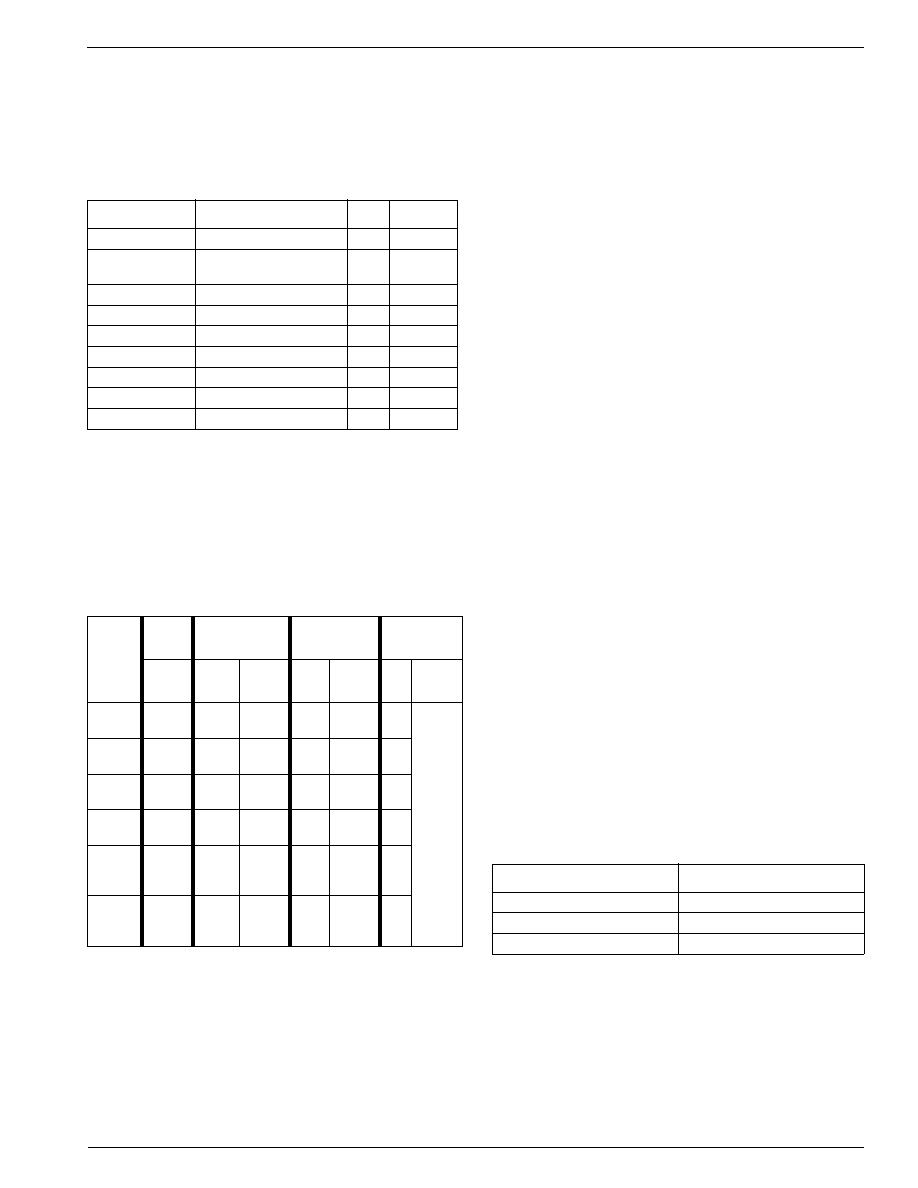
Table 12-7. Memory Interface Signal Pins
Name
Function
I/O
Active...
MM_CLK[1:0]
Memory bus clock
O
High
MM_CS#[3..0]
Chip selects for the four
memory ranks
O
Low
MM_RAS#
Row-address strobe
O
Low
MM_CAS#
Column address strobe
O
Low
MM_WE#
Write enable
O
Low
MM_A[13:0]
Address
O
High
MM_CKE[1:0]
Clock enable
O
High
MM_DQM[3:0]
Byte enables for dq bus
O
High
MM_DQ[31:0]
Bi-directional data bus
I/O
High
Table 12-8. Address Mapping Based on Rank Size
Rank
Size
Rank
Addr.
Row
Address
Column
Address
Bank
Address
H.Way
Bits
Pins
H.Way
Bits
Pins
H.Way
Bits
Pin
H.Way
Bit
512 KB
20-19
8,
6–0
18,
17–11
7–0
10–6,
4–2
9
5
1 MB
21-20
8–0
19–11
7–0
10–6,
4–2
2 MB
22-21
9–0
20–11
7–0
10–6,
4–2
10
4 MB
23–22
10–0
21–11
7–0
10–6,
4–2
11
8 MB
24-23
12,
10–0
11,
22–12
12,
8–0
11,
11–6,
4–2
11
16 MB
25-24
13-12
10–0
12-11,
23–13
12,
9–0
11,
12–6,
4–2
11
Table 12-9. SDRAM Mode Register Settings
Parameter
Value
Burst length
4
Wrap type
Interleaved
CAS latency
3
相關(guān)PDF資料 |
PDF描述 |
|---|---|
| 935266917557 | SPECIALTY CONSUMER CIRCUIT, PBGA292 |
| 935268386557 | SPECIALTY CONSUMER CIRCUIT, PBGA292 |
| 935267050025 | SPECIALTY CONSUMER CIRCUIT, UUC |
| 935267053005 | SPECIALTY CONSUMER CIRCUIT, UUC |
| 935267052005 | SPECIALTY CONSUMER CIRCUIT, UUC |
相關(guān)代理商/技術(shù)參數(shù) |
參數(shù)描述 |
|---|---|
| 935267356112 | 制造商:NXP Semiconductors 功能描述:IC TEA1507PN |
| 935268081112 | 制造商:NXP Semiconductors 功能描述:SUB ONLY IC |
| 935268721125 | 制造商:NXP Semiconductors 功能描述:Buffer/Line Driver 1-CH Non-Inverting 3-ST CMOS 5-Pin TSSOP T/R |
| 935269304128 | 制造商:ST-Ericsson 功能描述:IC AUDIO CODEC W/TCH SCRN 48LQFP |
| 935269544557 | 制造商:NXP Semiconductors 功能描述:SUB ONLY TDA9587-2US1-V1.3 |
發(fā)布緊急采購,3分鐘左右您將得到回復(fù)。