- 您現(xiàn)在的位置:買賣IC網(wǎng) > PDF目錄36339 > 935266871557 (NXP SEMICONDUCTORS) SPECIALTY CONSUMER CIRCUIT, PBGA292 PDF資料下載
參數(shù)資料
| 型號(hào): | 935266871557 |
| 廠商: | NXP SEMICONDUCTORS |
| 元件分類: | 消費(fèi)家電 |
| 英文描述: | SPECIALTY CONSUMER CIRCUIT, PBGA292 |
| 封裝: | PLASTIC, SOT-553-1, BGA-292 |
| 文件頁(yè)數(shù): | 85/532頁(yè) |
| 文件大小: | 1895K |
| 代理商: | 935266871557 |
第1頁(yè)第2頁(yè)第3頁(yè)第4頁(yè)第5頁(yè)第6頁(yè)第7頁(yè)第8頁(yè)第9頁(yè)第10頁(yè)第11頁(yè)第12頁(yè)第13頁(yè)第14頁(yè)第15頁(yè)第16頁(yè)第17頁(yè)第18頁(yè)第19頁(yè)第20頁(yè)第21頁(yè)第22頁(yè)第23頁(yè)第24頁(yè)第25頁(yè)第26頁(yè)第27頁(yè)第28頁(yè)第29頁(yè)第30頁(yè)第31頁(yè)第32頁(yè)第33頁(yè)第34頁(yè)第35頁(yè)第36頁(yè)第37頁(yè)第38頁(yè)第39頁(yè)第40頁(yè)第41頁(yè)第42頁(yè)第43頁(yè)第44頁(yè)第45頁(yè)第46頁(yè)第47頁(yè)第48頁(yè)第49頁(yè)第50頁(yè)第51頁(yè)第52頁(yè)第53頁(yè)第54頁(yè)第55頁(yè)第56頁(yè)第57頁(yè)第58頁(yè)第59頁(yè)第60頁(yè)第61頁(yè)第62頁(yè)第63頁(yè)第64頁(yè)第65頁(yè)第66頁(yè)第67頁(yè)第68頁(yè)第69頁(yè)第70頁(yè)第71頁(yè)第72頁(yè)第73頁(yè)第74頁(yè)第75頁(yè)第76頁(yè)第77頁(yè)第78頁(yè)第79頁(yè)第80頁(yè)第81頁(yè)第82頁(yè)第83頁(yè)第84頁(yè)當(dāng)前第85頁(yè)第86頁(yè)第87頁(yè)第88頁(yè)第89頁(yè)第90頁(yè)第91頁(yè)第92頁(yè)第93頁(yè)第94頁(yè)第95頁(yè)第96頁(yè)第97頁(yè)第98頁(yè)第99頁(yè)第100頁(yè)第101頁(yè)第102頁(yè)第103頁(yè)第104頁(yè)第105頁(yè)第106頁(yè)第107頁(yè)第108頁(yè)第109頁(yè)第110頁(yè)第111頁(yè)第112頁(yè)第113頁(yè)第114頁(yè)第115頁(yè)第116頁(yè)第117頁(yè)第118頁(yè)第119頁(yè)第120頁(yè)第121頁(yè)第122頁(yè)第123頁(yè)第124頁(yè)第125頁(yè)第126頁(yè)第127頁(yè)第128頁(yè)第129頁(yè)第130頁(yè)第131頁(yè)第132頁(yè)第133頁(yè)第134頁(yè)第135頁(yè)第136頁(yè)第137頁(yè)第138頁(yè)第139頁(yè)第140頁(yè)第141頁(yè)第142頁(yè)第143頁(yè)第144頁(yè)第145頁(yè)第146頁(yè)第147頁(yè)第148頁(yè)第149頁(yè)第150頁(yè)第151頁(yè)第152頁(yè)第153頁(yè)第154頁(yè)第155頁(yè)第156頁(yè)第157頁(yè)第158頁(yè)第159頁(yè)第160頁(yè)第161頁(yè)第162頁(yè)第163頁(yè)第164頁(yè)第165頁(yè)第166頁(yè)第167頁(yè)第168頁(yè)第169頁(yè)第170頁(yè)第171頁(yè)第172頁(yè)第173頁(yè)第174頁(yè)第175頁(yè)第176頁(yè)第177頁(yè)第178頁(yè)第179頁(yè)第180頁(yè)第181頁(yè)第182頁(yè)第183頁(yè)第184頁(yè)第185頁(yè)第186頁(yè)第187頁(yè)第188頁(yè)第189頁(yè)第190頁(yè)第191頁(yè)第192頁(yè)第193頁(yè)第194頁(yè)第195頁(yè)第196頁(yè)第197頁(yè)第198頁(yè)第199頁(yè)第200頁(yè)第201頁(yè)第202頁(yè)第203頁(yè)第204頁(yè)第205頁(yè)第206頁(yè)第207頁(yè)第208頁(yè)第209頁(yè)第210頁(yè)第211頁(yè)第212頁(yè)第213頁(yè)第214頁(yè)第215頁(yè)第216頁(yè)第217頁(yè)第218頁(yè)第219頁(yè)第220頁(yè)第221頁(yè)第222頁(yè)第223頁(yè)第224頁(yè)第225頁(yè)第226頁(yè)第227頁(yè)第228頁(yè)第229頁(yè)第230頁(yè)第231頁(yè)第232頁(yè)第233頁(yè)第234頁(yè)第235頁(yè)第236頁(yè)第237頁(yè)第238頁(yè)第239頁(yè)第240頁(yè)第241頁(yè)第242頁(yè)第243頁(yè)第244頁(yè)第245頁(yè)第246頁(yè)第247頁(yè)第248頁(yè)第249頁(yè)第250頁(yè)第251頁(yè)第252頁(yè)第253頁(yè)第254頁(yè)第255頁(yè)第256頁(yè)第257頁(yè)第258頁(yè)第259頁(yè)第260頁(yè)第261頁(yè)第262頁(yè)第263頁(yè)第264頁(yè)第265頁(yè)第266頁(yè)第267頁(yè)第268頁(yè)第269頁(yè)第270頁(yè)第271頁(yè)第272頁(yè)第273頁(yè)第274頁(yè)第275頁(yè)第276頁(yè)第277頁(yè)第278頁(yè)第279頁(yè)第280頁(yè)第281頁(yè)第282頁(yè)第283頁(yè)第284頁(yè)第285頁(yè)第286頁(yè)第287頁(yè)第288頁(yè)第289頁(yè)第290頁(yè)第291頁(yè)第292頁(yè)第293頁(yè)第294頁(yè)第295頁(yè)第296頁(yè)第297頁(yè)第298頁(yè)第299頁(yè)第300頁(yè)第301頁(yè)第302頁(yè)第303頁(yè)第304頁(yè)第305頁(yè)第306頁(yè)第307頁(yè)第308頁(yè)第309頁(yè)第310頁(yè)第311頁(yè)第312頁(yè)第313頁(yè)第314頁(yè)第315頁(yè)第316頁(yè)第317頁(yè)第318頁(yè)第319頁(yè)第320頁(yè)第321頁(yè)第322頁(yè)第323頁(yè)第324頁(yè)第325頁(yè)第326頁(yè)第327頁(yè)第328頁(yè)第329頁(yè)第330頁(yè)第331頁(yè)第332頁(yè)第333頁(yè)第334頁(yè)第335頁(yè)第336頁(yè)第337頁(yè)第338頁(yè)第339頁(yè)第340頁(yè)第341頁(yè)第342頁(yè)第343頁(yè)第344頁(yè)第345頁(yè)第346頁(yè)第347頁(yè)第348頁(yè)第349頁(yè)第350頁(yè)第351頁(yè)第352頁(yè)第353頁(yè)第354頁(yè)第355頁(yè)第356頁(yè)第357頁(yè)第358頁(yè)第359頁(yè)第360頁(yè)第361頁(yè)第362頁(yè)第363頁(yè)第364頁(yè)第365頁(yè)第366頁(yè)第367頁(yè)第368頁(yè)第369頁(yè)第370頁(yè)第371頁(yè)第372頁(yè)第373頁(yè)第374頁(yè)第375頁(yè)第376頁(yè)第377頁(yè)第378頁(yè)第379頁(yè)第380頁(yè)第381頁(yè)第382頁(yè)第383頁(yè)第384頁(yè)第385頁(yè)第386頁(yè)第387頁(yè)第388頁(yè)第389頁(yè)第390頁(yè)第391頁(yè)第392頁(yè)第393頁(yè)第394頁(yè)第395頁(yè)第396頁(yè)第397頁(yè)第398頁(yè)第399頁(yè)第400頁(yè)第401頁(yè)第402頁(yè)第403頁(yè)第404頁(yè)第405頁(yè)第406頁(yè)第407頁(yè)第408頁(yè)第409頁(yè)第410頁(yè)第411頁(yè)第412頁(yè)第413頁(yè)第414頁(yè)第415頁(yè)第416頁(yè)第417頁(yè)第418頁(yè)第419頁(yè)第420頁(yè)第421頁(yè)第422頁(yè)第423頁(yè)第424頁(yè)第425頁(yè)第426頁(yè)第427頁(yè)第428頁(yè)第429頁(yè)第430頁(yè)第431頁(yè)第432頁(yè)第433頁(yè)第434頁(yè)第435頁(yè)第436頁(yè)第437頁(yè)第438頁(yè)第439頁(yè)第440頁(yè)第441頁(yè)第442頁(yè)第443頁(yè)第444頁(yè)第445頁(yè)第446頁(yè)第447頁(yè)第448頁(yè)第449頁(yè)第450頁(yè)第451頁(yè)第452頁(yè)第453頁(yè)第454頁(yè)第455頁(yè)第456頁(yè)第457頁(yè)第458頁(yè)第459頁(yè)第460頁(yè)第461頁(yè)第462頁(yè)第463頁(yè)第464頁(yè)第465頁(yè)第466頁(yè)第467頁(yè)第468頁(yè)第469頁(yè)第470頁(yè)第471頁(yè)第472頁(yè)第473頁(yè)第474頁(yè)第475頁(yè)第476頁(yè)第477頁(yè)第478頁(yè)第479頁(yè)第480頁(yè)第481頁(yè)第482頁(yè)第483頁(yè)第484頁(yè)第485頁(yè)第486頁(yè)第487頁(yè)第488頁(yè)第489頁(yè)第490頁(yè)第491頁(yè)第492頁(yè)第493頁(yè)第494頁(yè)第495頁(yè)第496頁(yè)第497頁(yè)第498頁(yè)第499頁(yè)第500頁(yè)第501頁(yè)第502頁(yè)第503頁(yè)第504頁(yè)第505頁(yè)第506頁(yè)第507頁(yè)第508頁(yè)第509頁(yè)第510頁(yè)第511頁(yè)第512頁(yè)第513頁(yè)第514頁(yè)第515頁(yè)第516頁(yè)第517頁(yè)第518頁(yè)第519頁(yè)第520頁(yè)第521頁(yè)第522頁(yè)第523頁(yè)第524頁(yè)第525頁(yè)第526頁(yè)第527頁(yè)第528頁(yè)第529頁(yè)第530頁(yè)第531頁(yè)第532頁(yè)
PRODUCT SPECIFICATION
12-1
SDRAM Memory System
Chapter 12
by Eino Jacobs, Chris Nelson, Thorwald Rabeler, Luis Lucas
12.1
NEW IN TM1300
Support of 64-Mbit SDRAMs organized in x16 and
128-Mbit organized in x32.
Partial support of 64-Mbit SDRAMs organized in x8
and 128-Mbit SDRAMs organized in x16.
External MM_MATCHOUT to MM_MATCHIN line is
no longer required.
12.2
TM1300 MAIN MEMORY OVERVIEW
TM1300 connects to its local memory system with a ded-
icated memory bus, shown in Figure 12-1. This bus inter-
faces only with SDRAM or SGRAM (synchronous graph-
ics DRAM) with its DSF pin tied low; TM1300 is the only
master on this bus.
A variety of device types, speeds, and rank1 sizes are
supported allowing a wide range of TM1300 systems to
be built. Table 12-1 summarizes the memory system fea-
tures.
The main memory interface provides all control and data
signals with sufficient drive capacity for a glueless con-
nection to a 143-MHz memory system with up to four
memory devices. Note that memory-system speed can
be different from TM1300 core speed; the ratio between
the memory system clock and TM1300 core clock is pro-
grammable.
With current memory technology, TM1300 supports a
glueless memory interface of up to 32 MBytes with four
4
×1M×16 SDRAM chips (four devices with 4 banks of
one million words, each 16 bits wide) or four 4x512Kx32
or two 8
×1M×16 SDRAM devices. Larger memories re-
quire a lower memory system clock frequency (though
the TM1300 core clock can be higher).
12.3
MAIN-MEMORY ADDRESS
APERTURE
TM1300’s local main memory is just one of three aper-
tures into the 4-GB address space of the DSPCPU:
SDRAM (0.5 to 64 MB in size),
MMIO (2 MB in size), and
PCI (any address not in SDRAM or MMIO).
MMIO registers control the positions of the address-
space apertures. The SDRAM aperture begins at the ab-
solute
address
specified
in
the
MMIO
register
DRAM_BASE and extends upward to the address spec-
ified in the DRAM_LIMIT register. If the SDRAM aperture
overlaps the memory hole, the memory hole is ignored.
The
MMIO
aperture
begins
at
the
address
in
MMIO_BASE, which defaults to 0xEFE00000 after pow-
er-up, and extends upwards 2 MB. (See Chapter 3,
“DSPCPU Architecture,” for a detailed discussion.) All
addresses that fall outside these two apertures are as-
sumed to be part of the PCI address aperture.
1.
In this document, the term ‘rank’ is used to refer to a
group of memory devices that are accessed together.
Historically, the term ‘bank’ has been used in this con-
text; to avoid confusion, this document uses bank to re-
fer to on-chip organization (SDRAM devices have two
or four internal banks) and rank to refer to off-chip, sys-
tem-level organization.
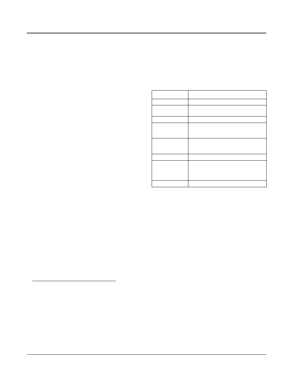
Table 12-1. Memory System Features
Characteristic
Comments
Data width
32 bits
Number of ranks
Four chip-select signals support up to
four ranks
Memory size
From 512 KB to 64 MB
Devices
supported
Jedec SGRAM (DSF tied low)
Jedec SDRAM (
×4, ×8, ×16, ×32)
PC100/133
Clock rate
Up to 143 MHz SDRAM speed (program-
mable ratio between TM1300 core clock
and memory system clock)
Bandwidth
572 MB/sec (at 143 MHz)
Glueless interface
Up to 4 chips at 143 MHz (e.g., 32 MB
memory with 4x512Kx32 SDRAM)
Up to 8 chips at 133 MHz (e.g., 64 MB
memory with 4x1Mx16 SDRAM)
Signal levels
3.3-V LVTTL
相關(guān)PDF資料 |
PDF描述 |
|---|---|
| 935266917557 | SPECIALTY CONSUMER CIRCUIT, PBGA292 |
| 935268386557 | SPECIALTY CONSUMER CIRCUIT, PBGA292 |
| 935267050025 | SPECIALTY CONSUMER CIRCUIT, UUC |
| 935267053005 | SPECIALTY CONSUMER CIRCUIT, UUC |
| 935267052005 | SPECIALTY CONSUMER CIRCUIT, UUC |
相關(guān)代理商/技術(shù)參數(shù) |
參數(shù)描述 |
|---|---|
| 935267356112 | 制造商:NXP Semiconductors 功能描述:IC TEA1507PN |
| 935268081112 | 制造商:NXP Semiconductors 功能描述:SUB ONLY IC |
| 935268721125 | 制造商:NXP Semiconductors 功能描述:Buffer/Line Driver 1-CH Non-Inverting 3-ST CMOS 5-Pin TSSOP T/R |
| 935269304128 | 制造商:ST-Ericsson 功能描述:IC AUDIO CODEC W/TCH SCRN 48LQFP |
| 935269544557 | 制造商:NXP Semiconductors 功能描述:SUB ONLY TDA9587-2US1-V1.3 |
發(fā)布緊急采購(gòu),3分鐘左右您將得到回復(fù)。