- 您現(xiàn)在的位置:買賣IC網(wǎng) > PDF目錄98011 > MC68306PV16 (FREESCALE SEMICONDUCTOR INC) 32-BIT, 16.67 MHz, MICROPROCESSOR, PQFP144 PDF資料下載
參數(shù)資料
| 型號(hào): | MC68306PV16 |
| 廠商: | FREESCALE SEMICONDUCTOR INC |
| 元件分類: | 微控制器/微處理器 |
| 英文描述: | 32-BIT, 16.67 MHz, MICROPROCESSOR, PQFP144 |
| 封裝: | PLASTIC, TQFP-144 |
| 文件頁(yè)數(shù): | 6/191頁(yè) |
| 文件大小: | 1311K |
| 代理商: | MC68306PV16 |
第1頁(yè)第2頁(yè)第3頁(yè)第4頁(yè)第5頁(yè)當(dāng)前第6頁(yè)第7頁(yè)第8頁(yè)第9頁(yè)第10頁(yè)第11頁(yè)第12頁(yè)第13頁(yè)第14頁(yè)第15頁(yè)第16頁(yè)第17頁(yè)第18頁(yè)第19頁(yè)第20頁(yè)第21頁(yè)第22頁(yè)第23頁(yè)第24頁(yè)第25頁(yè)第26頁(yè)第27頁(yè)第28頁(yè)第29頁(yè)第30頁(yè)第31頁(yè)第32頁(yè)第33頁(yè)第34頁(yè)第35頁(yè)第36頁(yè)第37頁(yè)第38頁(yè)第39頁(yè)第40頁(yè)第41頁(yè)第42頁(yè)第43頁(yè)第44頁(yè)第45頁(yè)第46頁(yè)第47頁(yè)第48頁(yè)第49頁(yè)第50頁(yè)第51頁(yè)第52頁(yè)第53頁(yè)第54頁(yè)第55頁(yè)第56頁(yè)第57頁(yè)第58頁(yè)第59頁(yè)第60頁(yè)第61頁(yè)第62頁(yè)第63頁(yè)第64頁(yè)第65頁(yè)第66頁(yè)第67頁(yè)第68頁(yè)第69頁(yè)第70頁(yè)第71頁(yè)第72頁(yè)第73頁(yè)第74頁(yè)第75頁(yè)第76頁(yè)第77頁(yè)第78頁(yè)第79頁(yè)第80頁(yè)第81頁(yè)第82頁(yè)第83頁(yè)第84頁(yè)第85頁(yè)第86頁(yè)第87頁(yè)第88頁(yè)第89頁(yè)第90頁(yè)第91頁(yè)第92頁(yè)第93頁(yè)第94頁(yè)第95頁(yè)第96頁(yè)第97頁(yè)第98頁(yè)第99頁(yè)第100頁(yè)第101頁(yè)第102頁(yè)第103頁(yè)第104頁(yè)第105頁(yè)第106頁(yè)第107頁(yè)第108頁(yè)第109頁(yè)第110頁(yè)第111頁(yè)第112頁(yè)第113頁(yè)第114頁(yè)第115頁(yè)第116頁(yè)第117頁(yè)第118頁(yè)第119頁(yè)第120頁(yè)第121頁(yè)第122頁(yè)第123頁(yè)第124頁(yè)第125頁(yè)第126頁(yè)第127頁(yè)第128頁(yè)第129頁(yè)第130頁(yè)第131頁(yè)第132頁(yè)第133頁(yè)第134頁(yè)第135頁(yè)第136頁(yè)第137頁(yè)第138頁(yè)第139頁(yè)第140頁(yè)第141頁(yè)第142頁(yè)第143頁(yè)第144頁(yè)第145頁(yè)第146頁(yè)第147頁(yè)第148頁(yè)第149頁(yè)第150頁(yè)第151頁(yè)第152頁(yè)第153頁(yè)第154頁(yè)第155頁(yè)第156頁(yè)第157頁(yè)第158頁(yè)第159頁(yè)第160頁(yè)第161頁(yè)第162頁(yè)第163頁(yè)第164頁(yè)第165頁(yè)第166頁(yè)第167頁(yè)第168頁(yè)第169頁(yè)第170頁(yè)第171頁(yè)第172頁(yè)第173頁(yè)第174頁(yè)第175頁(yè)第176頁(yè)第177頁(yè)第178頁(yè)第179頁(yè)第180頁(yè)第181頁(yè)第182頁(yè)第183頁(yè)第184頁(yè)第185頁(yè)第186頁(yè)第187頁(yè)第188頁(yè)第189頁(yè)第190頁(yè)第191頁(yè)
MOTOROLA
MC68306 USER'S MANUAL
5- 13
68306 regains bus ownership. Only one refresh cycle occurs after bus ownership is
regained, regardless of the time the bus was granted away.
The DRAM controller provides RAS/CAS timing, 15 multiplexed address bits, and refresh
timing. All DRAM accesses are either zero or one wait state cycles, unless delayed by a
refresh. Zero wait state operation supports DRAMs up to 80 ns RAS access, and one wait
state cycles supports DRAMs up to 120 ns RAS access (at 16.67 MHz). External DTACK
is not allowed on DRAM accesses. A refresh can add up to three extra wait-states to zero
wait-state accesses or 4 extra wait-states to one-wait state accesses. Read-modify-write
cycles to DRAM use page mode, and the write portion is always zero wait-state,
regardless of the DRDT bit setting.
The organization of external DRAM is one or two banks, by two bytes. CAS0 controls the
high byte (D15–D8) and CAS1 controls the low byte (D7–D0).
The minimum bank size is 128 Kbytes (64K
× 2 bytes), because of the address
multiplexer, shown in Table 5-3.
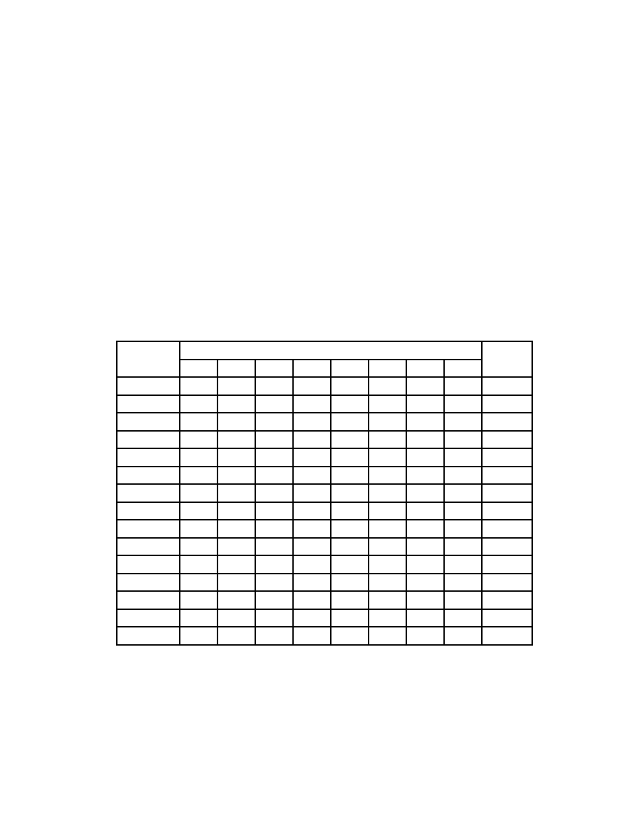
Table 5-3. DRAM Address Multiplexer
Value Of:
At RAS When DRSZ2–0 Is:
At CAS:
111
110
101
100
011
010
001
000
DRAMA14
A30
A29
A28
A27
A26
A25
A24
A23
A15
DRAMA13
A29
A28
A27
A26
A25
A24
A23
A22
A14
DRAMA12
A28
A27
A26
A25
A24
A23
A22
A21
A13
DRAMA11
A27
A26
A25
A24
A23
A22
A21
A20
A12
DRAMA10
A26
A25
A24
A23
A22
A21
A20
A19
A11
DRAMA9
A25
A24
A23
A22
A21
A20
A19
A18
A10
DRAMA8
A24
A23
A22
A21
A20
A19
A18
A17
A9
DRAMA7
A23
A22
A21
A20
A19
A18
A17
A16
A8
DRAMA6
A22
A21
A20
A19
A18
A17
A16
A15
A7
DRAMA5
A21
A20
A19
A18
A17
A16
A15
A14
A6
DRAMA4
A20
A19
A18
A17
A16
A15
A14
A13
A5
DRAMA3
A19
A18
A17
A16
A15
A14
A13
A12
A4
DRAMA2
A18
A17
A16
A15
A14
A13
A12
A11
A3
DRAMA1
A17
A16
A15
A14
A13
A12
A11
A10
A2
DRAMA0
A16
A15
A14
A13
A12
A11
A10
A9
A1
Because the DRAM address multiplexer provides contiguous address bits to the full 15-bit
DRAMA bus width during RAS, more banks can be supported by externally decoding bits
beyond the RAS address width of the DRAMs. If this is done, the DRAMA, CAS, and
DRAMW signals should be buffered. This will almost certainly require the wait state. Also,
DRAMs with more row address pins than column address pins are supported.
F
re
e
sc
a
le
S
e
m
ic
o
n
d
u
c
to
r,
I
Freescale Semiconductor, Inc.
For More Information On This Product,
Go to: www.freescale.com
n
c
..
.
相關(guān)PDF資料 |
PDF描述 |
|---|---|
| MC68450LC-8 | 4 CHANNEL(S), 8 MHz, DMA CONTROLLER, CDIP64 |
| MC68681L | 2 CHANNEL(S), 1M bps, SERIAL COMM CONTROLLER, CDIP40 |
| MC68681P | 2 CHANNEL(S), 1M bps, SERIAL COMM CONTROLLER, PDIP40 |
| MC68838FCC | 1 CHANNEL(S), 125M bps, FDDI CONTROLLER, CQFP120 |
| MC68EC020FG | 32-BIT, 25 MHz, MICROCONTROLLER, PQFP100 |
相關(guān)代理商/技術(shù)參數(shù) |
參數(shù)描述 |
|---|---|
| MC68306PV20B | 制造商:Rochester Electronics LLC 功能描述:INTEGRATED EC000 MPU - Bulk |
| MC68307 | 制造商:MOTOROLA 制造商全稱:Motorola, Inc 功能描述:Technical Summary Integrated Multiple-Bus Processor |
| MC68307AD | 制造商:MOTOROLA 制造商全稱:Motorola, Inc 功能描述:Technical Summary Integrated Multiple-Bus Processor |
| MC68307UM | 制造商:MOTOROLA 制造商全稱:Motorola, Inc 功能描述:Technical Summary Integrated Multiple-Bus Processor |
| MC68307V | 制造商:MOTOROLA 制造商全稱:Motorola, Inc 功能描述:Technical Summary Integrated Multiple-Bus Processor |
發(fā)布緊急采購(gòu),3分鐘左右您將得到回復(fù)。