- 您現(xiàn)在的位置:買賣IC網(wǎng) > PDF目錄1996 > HMC704LP4E (Hittite Microwave Corporation)IC FRACT-N PLL 16BIT 24QFN PDF資料下載
參數(shù)資料
| 型號(hào): | HMC704LP4E |
| 廠商: | Hittite Microwave Corporation |
| 文件頁(yè)數(shù): | 16/44頁(yè) |
| 文件大?。?/td> | 0K |
| 描述: | IC FRACT-N PLL 16BIT 24QFN |
| 標(biāo)準(zhǔn)包裝: | 1 |
| 類型: | 整數(shù) N/小數(shù) N 分頻 |
| PLL: | 是 |
| 輸入: | CMOS |
| 輸出: | CMOS |
| 電路數(shù): | 1 |
| 比率 - 輸入:輸出: | 1:1 |
| 差分 - 輸入:輸出: | 是/無(wú) |
| 頻率 - 最大: | 8GHz |
| 除法器/乘法器: | 是/無(wú) |
| 電源電壓: | 3.3V,5V |
| 工作溫度: | -40°C ~ 85°C |
| 安裝類型: | 表面貼裝 |
| 封裝/外殼: | 24-VQFN 裸露焊盤 |
| 供應(yīng)商設(shè)備封裝: | 24-QFN 裸露焊盤(4x4) |
| 包裝: | 標(biāo)準(zhǔn)包裝 |
| 其它名稱: | 1127-1066-6 |
第1頁(yè)第2頁(yè)第3頁(yè)第4頁(yè)第5頁(yè)第6頁(yè)第7頁(yè)第8頁(yè)第9頁(yè)第10頁(yè)第11頁(yè)第12頁(yè)第13頁(yè)第14頁(yè)第15頁(yè)當(dāng)前第16頁(yè)第17頁(yè)第18頁(yè)第19頁(yè)第20頁(yè)第21頁(yè)第22頁(yè)第23頁(yè)第24頁(yè)第25頁(yè)第26頁(yè)第27頁(yè)第28頁(yè)第29頁(yè)第30頁(yè)第31頁(yè)第32頁(yè)第33頁(yè)第34頁(yè)第35頁(yè)第36頁(yè)第37頁(yè)第38頁(yè)第39頁(yè)第40頁(yè)第41頁(yè)第42頁(yè)第43頁(yè)第44頁(yè)
P
LL
s
-
s
M
T
5 - 23
HMC704LP4E
v03.1211
8 GHz fractionaL-n PLL
For price, delivery, and to place orders: Hittite Microwave Corporation,20 Alpha Road, Chelmsford, MA 01824
Phone: 978-250-3343
Fax: 978-250-3373
Order On-line at www.hittite.com
Application Support: Phone: 978-250-3343 or apps@hittite.com
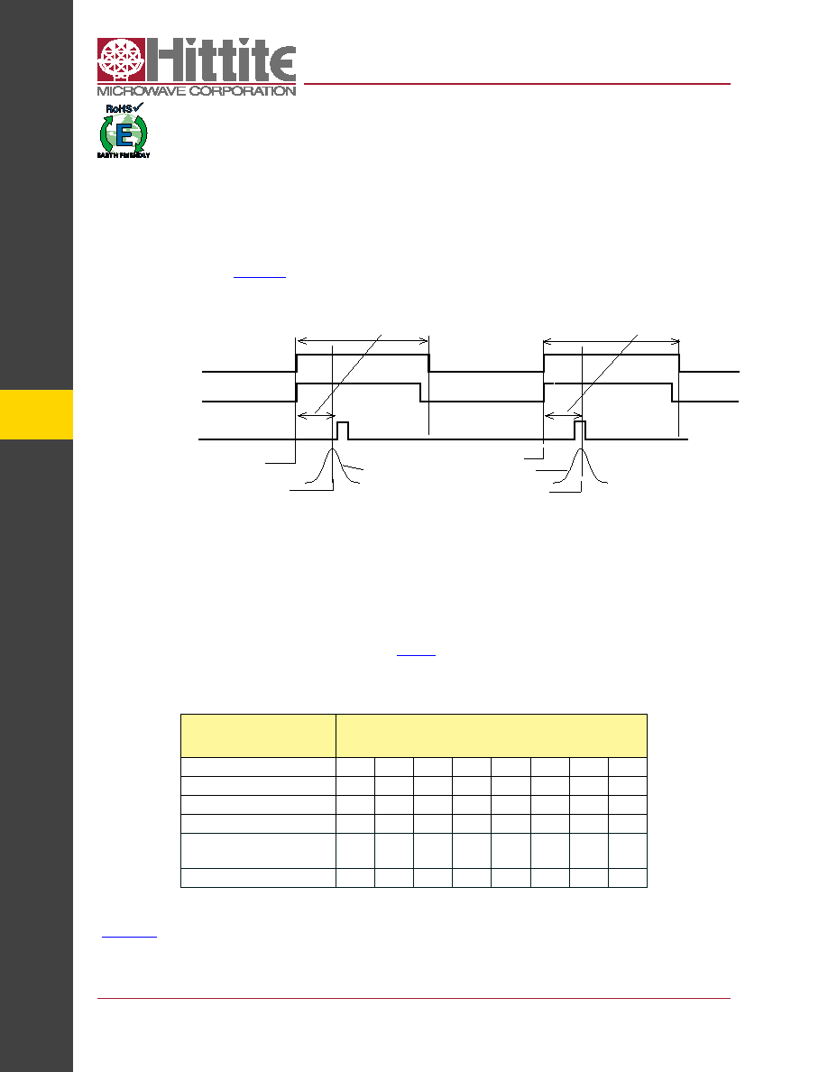
Lock Detect operation with Phase offset
When operating in fractional mode the linearity of the charge pump and phase detector are much more critical than in
integer mode. The phase detector linearity degrades when operated with zero phase offset. Hence in fractional mode it
is necessary to offset the phase of the reference and VCO at the phase detector. In such a case, for example with an
offset delay, as shown in Figure 32, the VCO arrival may always occur after the reference. The lock detect circuit win-
dow may need to be adjusted to allow for the delay being used, if the delay is large.
VCO AT PD with FRAC Jitter
LOCK
DETECT
WINDOW
Twindow ~ +10nsec
Figure 32. Lock Detect Window - Fractional Mode with Offset
REF PHAsE ARRIVAL
FRACTIONAL MODE
VCO ARRIVAL DIsTRIBUTION AT PD
PHAsE JITTER
LOCK WINDOW
AVG VCO PHAsE OFFsET
AVG PHAsE OFFsET
FRACTIONAL MODE
AVG VCO PHAsE OFFsET
REF PHAsE ARRIVAL
AVG PHAsE OFFsET
AT PD
In integer mode, 0 offset is recommended. In fractional mode, the time offset should be set to ~ 2.5ns + 4Tps, where Tps
is the RF period at the fractional prescaler input (i.e. after the optional fixed divide by 2). Refer to the Fractional Opera-
tion section for further details about calculating charge pump offset currents
Digital Lock Detect with Digital Window Example
Typical Digital Lock detect window widths are shown in Table 7. Lock Detect windows typically vary +/-10% vs voltage
and +/-15% over -40C to +85C.
table 7. typical Digital Lock Detect Window
LD Timer speed
Reg07[11:10]
Digital Lock Detect Window
Nominal Value +/-25%
(nsec)
Fastest 00
6.5
8.0
11.0
17
29
53
100
195
01
7.0
8.9
12.8
21
36
68
130
255
10
7.1
9.2
13.3
22
38
72
138
272
slowest 11
7.6
10.2
15.4
26
47
88
172
338
LD Timer Divider setting
Reg07[9:7]
0
1
2
3
4
5
6
7
LD Timer Divider Value
0.5
1
2
4
8
16
32
64
As an example if we operate in fractional mode, with a 50MHz PD, a 2700 MHz VCO and a Charge pump gain of 2mA
(“Reg 09h”), based on the previous example, we should set the DC phase offset near 2.5ns+4x370ps =4ns, or 20% of
the 20ns reference period. It becomes a larger proportion with increasing fpd. The offset current is therefore 20% x
2mA=400uA. The polarity of the offset should be chosen so that the VCO lags the reference for the most consistent
results. For non-inverting /inverting loop filter configurations, we recommend down/up offsets, respectively.
REFERENCE
sIGNAL
相關(guān)PDF資料 |
PDF描述 |
|---|---|
| HMC830LP6GE | IC FRACT-N PLL W/VCO 40QFN |
| HMP8117CNZ | IC VIDEO DECODER NTSC/PAL 80PQFP |
| HMP8156ACNZ | IC VIDEO ENCODER NTSC/PAL 64MQFP |
| HSP45102SC-40Z | IC OSC NCO 40MHZ 28-SOIC |
| HSP45106JC-33Z | IC OSC NCO 33MHZ 84-PLCC |
相關(guān)代理商/技術(shù)參數(shù) |
參數(shù)描述 |
|---|---|
| HMC704LP4ETR | 制造商:Hittite Microwave Corp 功能描述:IC FRACT-N PLL 16BIT 24QFN |
| HMC705LP4 | 制造商:HITTITE 制造商全稱:Hittite Microwave Corporation 功能描述:6.5 GHz PROGRAMMABLE DIVIDER (N = 1 - 17) |
| HMC705LP4E | 制造商:Hittite Microwave Corp 功能描述:IC DIVIDER HBT PROGR 24-QFN |
| HMC705LP4ETR | 功能描述:IC DIVIDER HBT PROGR 24QFN 制造商:analog devices inc. 系列:- 包裝:剪切帶(CT) 零件狀態(tài):在售 功能:分頻器 頻率:100MHz ~ 6.5GHz RF 類型:- 輔助屬性:- 封裝/外殼:24-VFQFN 裸露焊盤 供應(yīng)商器件封裝:24-QFN(4x4) 標(biāo)準(zhǔn)包裝:1 |
| hmc706lc3c | 制造商:Hittite Microwave Corp 功能描述:IC CONV NRZ-RZ 13GBPS 16SMD |
發(fā)布緊急采購(gòu),3分鐘左右您將得到回復(fù)。