- 您現(xiàn)在的位置:買賣IC網(wǎng) > PDF目錄36339 > 935266917557 (NXP SEMICONDUCTORS) SPECIALTY CONSUMER CIRCUIT, PBGA292 PDF資料下載
參數(shù)資料
| 型號: | 935266917557 |
| 廠商: | NXP SEMICONDUCTORS |
| 元件分類: | 消費家電 |
| 英文描述: | SPECIALTY CONSUMER CIRCUIT, PBGA292 |
| 封裝: | PLASTIC, SOT-553-1, BGA-292 |
| 文件頁數(shù): | 335/532頁 |
| 文件大小: | 1895K |
| 代理商: | 935266917557 |
第1頁第2頁第3頁第4頁第5頁第6頁第7頁第8頁第9頁第10頁第11頁第12頁第13頁第14頁第15頁第16頁第17頁第18頁第19頁第20頁第21頁第22頁第23頁第24頁第25頁第26頁第27頁第28頁第29頁第30頁第31頁第32頁第33頁第34頁第35頁第36頁第37頁第38頁第39頁第40頁第41頁第42頁第43頁第44頁第45頁第46頁第47頁第48頁第49頁第50頁第51頁第52頁第53頁第54頁第55頁第56頁第57頁第58頁第59頁第60頁第61頁第62頁第63頁第64頁第65頁第66頁第67頁第68頁第69頁第70頁第71頁第72頁第73頁第74頁第75頁第76頁第77頁第78頁第79頁第80頁第81頁第82頁第83頁第84頁第85頁第86頁第87頁第88頁第89頁第90頁第91頁第92頁第93頁第94頁第95頁第96頁第97頁第98頁第99頁第100頁第101頁第102頁第103頁第104頁第105頁第106頁第107頁第108頁第109頁第110頁第111頁第112頁第113頁第114頁第115頁第116頁第117頁第118頁第119頁第120頁第121頁第122頁第123頁第124頁第125頁第126頁第127頁第128頁第129頁第130頁第131頁第132頁第133頁第134頁第135頁第136頁第137頁第138頁第139頁第140頁第141頁第142頁第143頁第144頁第145頁第146頁第147頁第148頁第149頁第150頁第151頁第152頁第153頁第154頁第155頁第156頁第157頁第158頁第159頁第160頁第161頁第162頁第163頁第164頁第165頁第166頁第167頁第168頁第169頁第170頁第171頁第172頁第173頁第174頁第175頁第176頁第177頁第178頁第179頁第180頁第181頁第182頁第183頁第184頁第185頁第186頁第187頁第188頁第189頁第190頁第191頁第192頁第193頁第194頁第195頁第196頁第197頁第198頁第199頁第200頁第201頁第202頁第203頁第204頁第205頁第206頁第207頁第208頁第209頁第210頁第211頁第212頁第213頁第214頁第215頁第216頁第217頁第218頁第219頁第220頁第221頁第222頁第223頁第224頁第225頁第226頁第227頁第228頁第229頁第230頁第231頁第232頁第233頁第234頁第235頁第236頁第237頁第238頁第239頁第240頁第241頁第242頁第243頁第244頁第245頁第246頁第247頁第248頁第249頁第250頁第251頁第252頁第253頁第254頁第255頁第256頁第257頁第258頁第259頁第260頁第261頁第262頁第263頁第264頁第265頁第266頁第267頁第268頁第269頁第270頁第271頁第272頁第273頁第274頁第275頁第276頁第277頁第278頁第279頁第280頁第281頁第282頁第283頁第284頁第285頁第286頁第287頁第288頁第289頁第290頁第291頁第292頁第293頁第294頁第295頁第296頁第297頁第298頁第299頁第300頁第301頁第302頁第303頁第304頁第305頁第306頁第307頁第308頁第309頁第310頁第311頁第312頁第313頁第314頁第315頁第316頁第317頁第318頁第319頁第320頁第321頁第322頁第323頁第324頁第325頁第326頁第327頁第328頁第329頁第330頁第331頁第332頁第333頁第334頁當前第335頁第336頁第337頁第338頁第339頁第340頁第341頁第342頁第343頁第344頁第345頁第346頁第347頁第348頁第349頁第350頁第351頁第352頁第353頁第354頁第355頁第356頁第357頁第358頁第359頁第360頁第361頁第362頁第363頁第364頁第365頁第366頁第367頁第368頁第369頁第370頁第371頁第372頁第373頁第374頁第375頁第376頁第377頁第378頁第379頁第380頁第381頁第382頁第383頁第384頁第385頁第386頁第387頁第388頁第389頁第390頁第391頁第392頁第393頁第394頁第395頁第396頁第397頁第398頁第399頁第400頁第401頁第402頁第403頁第404頁第405頁第406頁第407頁第408頁第409頁第410頁第411頁第412頁第413頁第414頁第415頁第416頁第417頁第418頁第419頁第420頁第421頁第422頁第423頁第424頁第425頁第426頁第427頁第428頁第429頁第430頁第431頁第432頁第433頁第434頁第435頁第436頁第437頁第438頁第439頁第440頁第441頁第442頁第443頁第444頁第445頁第446頁第447頁第448頁第449頁第450頁第451頁第452頁第453頁第454頁第455頁第456頁第457頁第458頁第459頁第460頁第461頁第462頁第463頁第464頁第465頁第466頁第467頁第468頁第469頁第470頁第471頁第472頁第473頁第474頁第475頁第476頁第477頁第478頁第479頁第480頁第481頁第482頁第483頁第484頁第485頁第486頁第487頁第488頁第489頁第490頁第491頁第492頁第493頁第494頁第495頁第496頁第497頁第498頁第499頁第500頁第501頁第502頁第503頁第504頁第505頁第506頁第507頁第508頁第509頁第510頁第511頁第512頁第513頁第514頁第515頁第516頁第517頁第518頁第519頁第520頁第521頁第522頁第523頁第524頁第525頁第526頁第527頁第528頁第529頁第530頁第531頁第532頁
TM1300 Data Book
Philips Semiconductors
1-16
PRODUCT SPECIFICATION
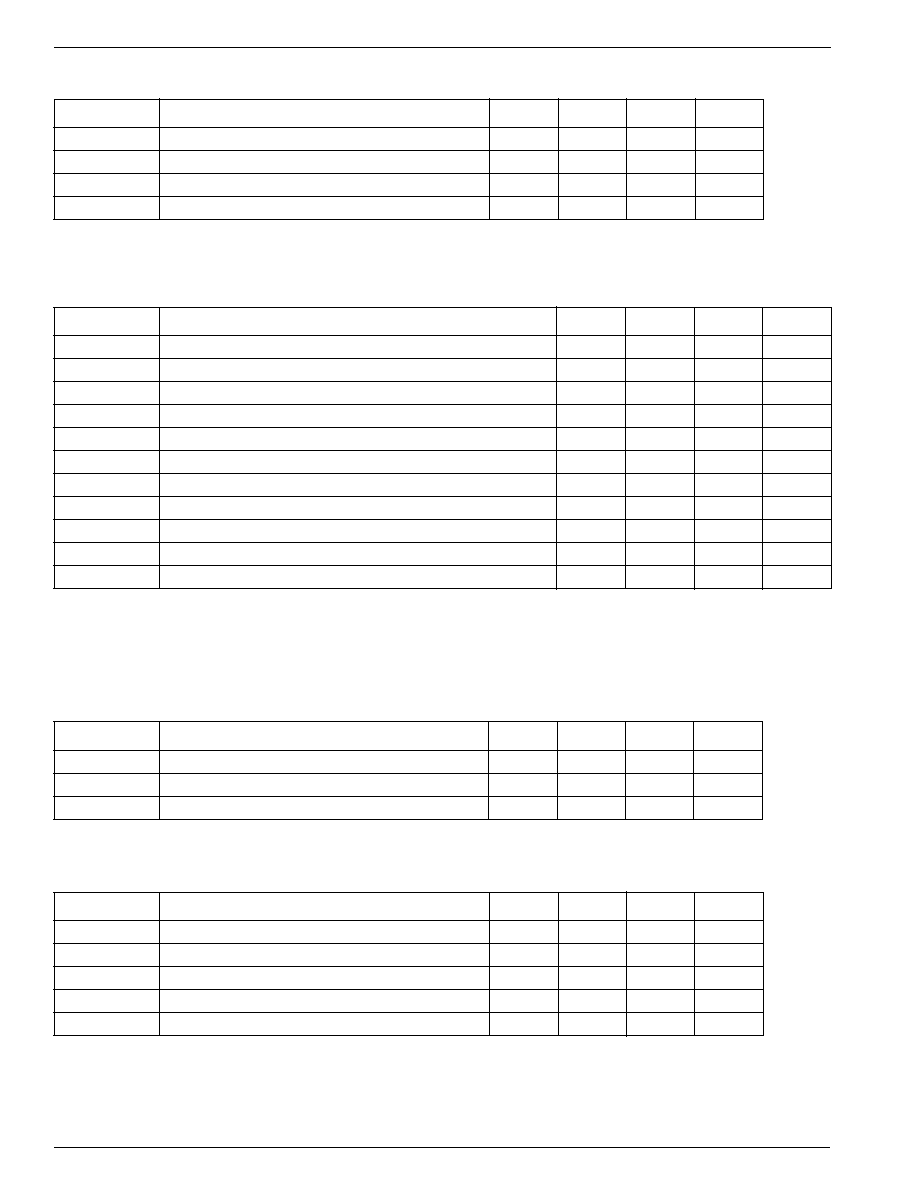
1.9.4.9
JTAG I/O timing
Notes:
1. See the timing measurement conditions in Figure 1-10.
2. See the timing measurement conditions in Figure 1-9.
1.9.4.10
I2C I/O timing
Notes:
1. See the timing measurement conditions in Figure 1-11.
2. See the timing measurement conditions in Figure 1-12.
3. See the timing measurement conditions in Figure 1-13.
4. See the timing measurement conditions in Figure 1-14.
5. See the timing measurement conditions in Figure 1-15.
1.9.4.11
Video In I/O Timing
Notes:
1. See the timing measurement conditions in Figure 1-16.
1.9.4.12
Video Out I/O Timing
Notes:
1. See the timing measurement conditions in Figure 1-17.
2. See the timing measurement conditions in Figure 1-18.
3. CLKOUT asserted, i.e. the VO unit is the source of VO_CLK
4. CLKOUT negated, i.e. the external world is the source of VO_CLK
Symbol
Parameter
Min.
Max
Units
Notes
fJTAG-CLK
JTAG clock frequency
20
MHz
Tclk-TDO
JTAG_TCK to JTAG_TDO valid delay
2
10
ns
1
Tsu-TCK
Input setup time to JTAG_TCK
3
ns
2
Th-TCK
Input hold time from JTAG_TCK
7
ns
2
Symbol
Parameter
Min.
Max
Units
Notes
fSCL
SCL clock frequency
400
kHz
1
TBUF
Bus free time
1
us
2
Tsu-STA
Start condition set up time
1
us
3
Th-STA
Start condition hold time
1
us
3
TLOW
SCL LOW time
1
us
1
THIGH
SCL HIGH time
1
us
1
Tf
SCL and SDA fall time (Cb = 10-400 pF, from VIH-IIC to VIL-IIC)
20+0.1Cb
250
ns
1
Tsu-SDA
Data setup time
100
ns
4
Th-SDA
Data hold time
0
ns
4
Tdv-SDA
SCL LOW to data out valid
0.5
us
5
Tdv-STO
SCL HIGH to data out
1
ns
5
Symbol
Parameter
Min.
Max
Units
Notes
fVI-CLK
Video In clock frequency
81
MHz
Tsu-CLK
Input setup time to VI_CLK
2
ns
1
Th-CLK
Input hold time from VI_CLK
2
ns
1
Symbol
Parameter
Min.
Max
Units
Notes
fVO-CLK
Video Out clock frequency
81
MHz
TCLK-DV
VO_CLK to VO_DATA (or VO_IO*) out
3
8.5
ns
1,3
TCLK-DV
VO_CLK to VO_DATA (or VO_IO*) out
3
8.5
ns
1,4
Tsu-CLK
VO_IO* setup time to VO_CLK
10
ns
2
Th-CLK
VO_IO* hold time from VO_CLK
3
ns
2
相關PDF資料 |
PDF描述 |
|---|---|
| 935268386557 | SPECIALTY CONSUMER CIRCUIT, PBGA292 |
| 935267050025 | SPECIALTY CONSUMER CIRCUIT, UUC |
| 935267053005 | SPECIALTY CONSUMER CIRCUIT, UUC |
| 935267052005 | SPECIALTY CONSUMER CIRCUIT, UUC |
| 935267395518 | COLOR SIGNAL DECODER, PBGA156 |
相關代理商/技術參數(shù) |
參數(shù)描述 |
|---|---|
| 935267356112 | 制造商:NXP Semiconductors 功能描述:IC TEA1507PN |
| 935268081112 | 制造商:NXP Semiconductors 功能描述:SUB ONLY IC |
| 935268721125 | 制造商:NXP Semiconductors 功能描述:Buffer/Line Driver 1-CH Non-Inverting 3-ST CMOS 5-Pin TSSOP T/R |
| 935269304128 | 制造商:ST-Ericsson 功能描述:IC AUDIO CODEC W/TCH SCRN 48LQFP |
| 935269544557 | 制造商:NXP Semiconductors 功能描述:SUB ONLY TDA9587-2US1-V1.3 |
發(fā)布緊急采購,3分鐘左右您將得到回復。