- 您現(xiàn)在的位置:買賣IC網(wǎng) > PDF目錄45052 > M66596WG UNIVERSAL SERIAL BUS CONTROLLER, PBGA64 PDF資料下載
參數(shù)資料
| 型號: | M66596WG |
| 元件分類: | 總線控制器 |
| 英文描述: | UNIVERSAL SERIAL BUS CONTROLLER, PBGA64 |
| 封裝: | 0.80 MM PITCH, FBGA-64 |
| 文件頁數(shù): | 110/133頁 |
| 文件大小: | 1611K |
| 代理商: | M66596WG |
第1頁第2頁第3頁第4頁第5頁第6頁第7頁第8頁第9頁第10頁第11頁第12頁第13頁第14頁第15頁第16頁第17頁第18頁第19頁第20頁第21頁第22頁第23頁第24頁第25頁第26頁第27頁第28頁第29頁第30頁第31頁第32頁第33頁第34頁第35頁第36頁第37頁第38頁第39頁第40頁第41頁第42頁第43頁第44頁第45頁第46頁第47頁第48頁第49頁第50頁第51頁第52頁第53頁第54頁第55頁第56頁第57頁第58頁第59頁第60頁第61頁第62頁第63頁第64頁第65頁第66頁第67頁第68頁第69頁第70頁第71頁第72頁第73頁第74頁第75頁第76頁第77頁第78頁第79頁第80頁第81頁第82頁第83頁第84頁第85頁第86頁第87頁第88頁第89頁第90頁第91頁第92頁第93頁第94頁第95頁第96頁第97頁第98頁第99頁第100頁第101頁第102頁第103頁第104頁第105頁第106頁第107頁第108頁第109頁當前第110頁第111頁第112頁第113頁第114頁第115頁第116頁第117頁第118頁第119頁第120頁第121頁第122頁第123頁第124頁第125頁第126頁第127頁第128頁第129頁第130頁第131頁第132頁第133頁
M66596FP/WG
rev .1.00
2006.3.14
page 76 of 127
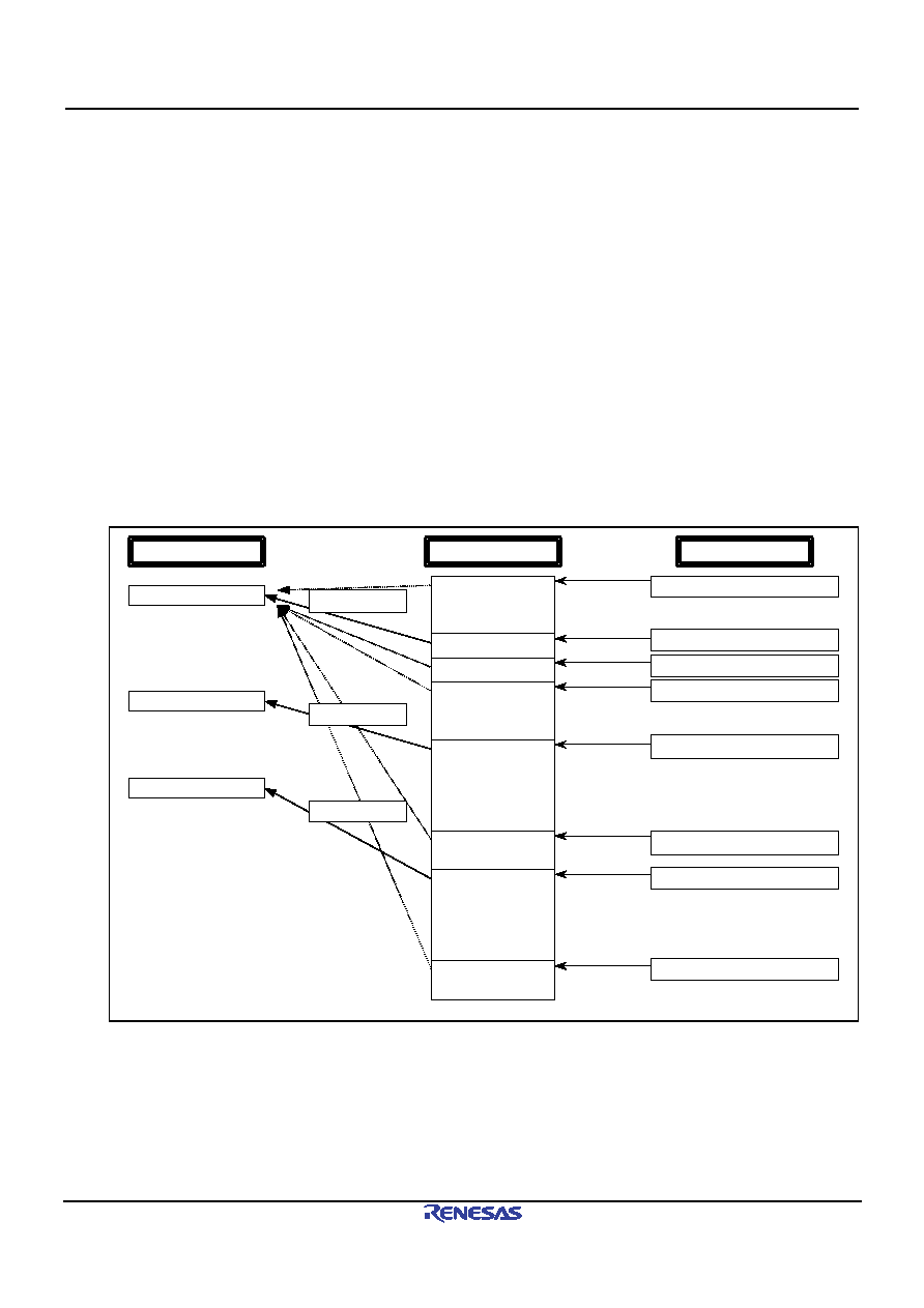
3.4 Buffer memory
This chapter explains operation about the buffer memory which this controller contains. When there is no
description, both a Host and Peripheral are the same operation.
3.4.1
Buffer memory allocation
Figure 3.19 shows an example of a buffer memory map for the controller. The buffer memory is an area shared by
the user system control CPU and the controller. In the buffer memory status, there are times when the access right
to the buffer memory is allocated to the user system (CPU side), and times when it is allocated to the controller (SIE
side).
The buffer memory sets independent areas for each pipe. In the memory areas, 64 bytes comprise one block, and
the memory areas are set using the first block number of the number of blocks (specified using the BUFNMB and
BUFSIZE
bits of the PIPEBUF register). Moreover, three FIFO ports are used for access to the buffer memory
(reading and writing data). A pipe is assigned to the FIFO port by specifying the pipe number using the CURPIPE
bit of the C/DxFIFOSEL register.
The buffer statuses of the various pipes can be confirmed using the BSTS bit of the DCPCTR register and
PIPExCTR
register. Also, the access right of the FIFO port can be confirmed using the FRDY bit of the C/DxFIFOCTR
register.
FIFO Port
D0FIFO Port
BUFNMB=0, BUFSIZE=3
CFIFO Port
D1FIFO Port
CURPIPE=1
CURPIPE=3
Buffer memory
PIPEBUF reg
PIPE0
PIPE6
PIPE7
PIPE5
PIPE1
PIPE2
PIPE3
PIPE4
BUFNMB=4, BUFSIZE=0
BUFNMB=5, BUFSIZE=0
BUFNMB=6, BUFSIZE=3
BUFNMB=10, BUFSIZE=7
BUFNMB=18, BUFSIZE=3
BUFNMB=22, BUFSIZE=7
BUFNMB=28, BUFSIZE=2
CURPIPE=6
Figure 3.19 Example of buffer memory map
相關PDF資料 |
PDF描述 |
|---|---|
| M6XXLFXI | OTHER CLOCK GENERATOR, QCC16 |
| M300LFXIT | 50 MHz, OTHER CLOCK GENERATOR, QCC16 |
| M74HC00C1R | HC/UH SERIES, QUAD 2-INPUT NAND GATE, PQCC20 |
| M74HC157B1N | HC/UH SERIES, QUAD 2 LINE TO 1 LINE MULTIPLEXER, TRUE OUTPUT, PDIP16 |
| M74HC158C1 | HC/UH SERIES, QUAD 2 LINE TO 1 LINE MULTIPLEXER, INVERTED OUTPUT, PQCC20 |
相關代理商/技術參數(shù) |
參數(shù)描述 |
|---|---|
| M66596WG#RB0Z | 制造商:Renesas Electronics 功能描述:Tray 制造商:Renesas 功能描述:0 |
| M6668 | 制造商:Tamura Corporation of America 功能描述: |
| M66700P | 制造商:MITSUBISHI 制造商全稱:Mitsubishi Electric Semiconductor 功能描述:DUAL HIGH-SPEED CCD CLOCK DRIVER |
| M66700WP | 制造商:MITSUBISHI 制造商全稱:Mitsubishi Electric Semiconductor 功能描述:DUAL HIGH-SPEED CCD CLOCK DRIVER |
| M66701P | 制造商:MITSUBISHI 制造商全稱:Mitsubishi Electric Semiconductor 功能描述:DUAL HIGH-SPEED CCD CLOCK DRIVER |
發(fā)布緊急采購,3分鐘左右您將得到回復。