- 您現(xiàn)在的位置:買賣IC網(wǎng) > PDF目錄45052 > M66596WG UNIVERSAL SERIAL BUS CONTROLLER, PBGA64 PDF資料下載
參數(shù)資料
| 型號: | M66596WG |
| 元件分類: | 總線控制器 |
| 英文描述: | UNIVERSAL SERIAL BUS CONTROLLER, PBGA64 |
| 封裝: | 0.80 MM PITCH, FBGA-64 |
| 文件頁數(shù): | 103/133頁 |
| 文件大?。?/td> | 1611K |
| 代理商: | M66596WG |
第1頁第2頁第3頁第4頁第5頁第6頁第7頁第8頁第9頁第10頁第11頁第12頁第13頁第14頁第15頁第16頁第17頁第18頁第19頁第20頁第21頁第22頁第23頁第24頁第25頁第26頁第27頁第28頁第29頁第30頁第31頁第32頁第33頁第34頁第35頁第36頁第37頁第38頁第39頁第40頁第41頁第42頁第43頁第44頁第45頁第46頁第47頁第48頁第49頁第50頁第51頁第52頁第53頁第54頁第55頁第56頁第57頁第58頁第59頁第60頁第61頁第62頁第63頁第64頁第65頁第66頁第67頁第68頁第69頁第70頁第71頁第72頁第73頁第74頁第75頁第76頁第77頁第78頁第79頁第80頁第81頁第82頁第83頁第84頁第85頁第86頁第87頁第88頁第89頁第90頁第91頁第92頁第93頁第94頁第95頁第96頁第97頁第98頁第99頁第100頁第101頁第102頁當(dāng)前第103頁第104頁第105頁第106頁第107頁第108頁第109頁第110頁第111頁第112頁第113頁第114頁第115頁第116頁第117頁第118頁第119頁第120頁第121頁第122頁第123頁第124頁第125頁第126頁第127頁第128頁第129頁第130頁第131頁第132頁第133頁
M66596FP/WG
rev .1.00
2006.3.14
page 69 of 127
3.2.7
Control transfer stage transition interrupt
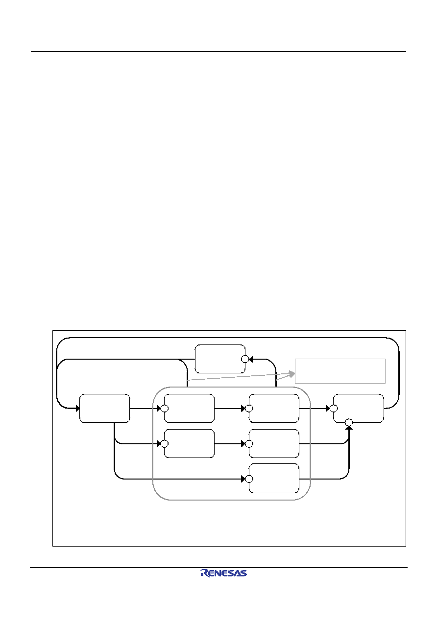
Figure 3.17 shows a diagram of how the controller handles the control transfer stage transition. In the Peripheral
mode, the controller controls the control transfer sequence and generates control transfer stage transition interrupts.
Control transfer stage transition interrupts can be enabled or disabled individually, using the INTENB0 register.
Also, the transfer stage that underwent a transition can be confirmed using the CTSQ bit of the INTSTS0 register.
The control transfer sequence errors are noted below. If an error occurs, the PID bit of the DCPCTR register goes to
“1X” (STALL).
(1)
During control read transfers
(a) At the IN token of the data stage, an OUT or PING token is received when there have been no data
transfers at all
(b) An IN token is received at the status stage
(c)
A packet is received at the status stage for which the data packet is "DATAPID=DATA0”
(2)
During control write transfers
(a) For the OUT token of the data stage, when there have been no ACK responses at all, the IN token is
received
(b) A packet is received at the data stage for which the first data packet is "DATAPID=DATA0"
(c)
At the status stage, an OUT or PING token is received
(3)
During control write no-data transfers
(a) At the status stage, an OUT or PING token is received
At the control write transfer stage, if the number of received data elements exceeds the wLength value of the USB
request, it cannot be recognized as a control transfer sequence error. Also, at the control read transfer status stage,
packets other than Zero-Length packets are received by an ACK response being carried out, and the transfer ends
normally.
If a CTRT interrupt occurs in response to a sequence error (“SERR=1”), the “CTSQ=110” value is held until
“CTRT=0” is written from the user system (the interrupt status is cleared). Because of this, while “CTSQ=110” is
being held, the CTRT interrupt that ends the setup stage will not be generated even if a new USB request is received.
(The controller holds the setup stage end, and after the interrupt status has been cleared by software, a setup stage
end interrupt is generated.)
ACK sent
ACK received
Error detected
Setup token
received
ACK sent
“CTSQ=011”
Control write data
stage
“CTSQ=100”
Control write status
stage
“CTSQ=000”
Idle stage
“CTSQ=101”
Control write
no-data status stage
OUT token
IN token
ACK received
1
3
4
“CTSQ=000”
Setup stage
“CTSQ=001”
Control read data
stage
“CTSQ=010”
Control read status
stage
2
1
4
“CTSQ=110”
Control transfer
sequence error
5
CTRT interrupts
1. Setup stage completed
2. Control read transfer status stage transition
3. Control write transfer status stage transition
4. Control transfer completed
5. Control transfer sequence error
Setup token received
If errors are detected at all stages in
the box, IN token reception is valid.
ACK sent
Figure 3.17 Control transfer stage transitions
相關(guān)PDF資料 |
PDF描述 |
|---|---|
| M6XXLFXI | OTHER CLOCK GENERATOR, QCC16 |
| M300LFXIT | 50 MHz, OTHER CLOCK GENERATOR, QCC16 |
| M74HC00C1R | HC/UH SERIES, QUAD 2-INPUT NAND GATE, PQCC20 |
| M74HC157B1N | HC/UH SERIES, QUAD 2 LINE TO 1 LINE MULTIPLEXER, TRUE OUTPUT, PDIP16 |
| M74HC158C1 | HC/UH SERIES, QUAD 2 LINE TO 1 LINE MULTIPLEXER, INVERTED OUTPUT, PQCC20 |
相關(guān)代理商/技術(shù)參數(shù) |
參數(shù)描述 |
|---|---|
| M66596WG#RB0Z | 制造商:Renesas Electronics 功能描述:Tray 制造商:Renesas 功能描述:0 |
| M6668 | 制造商:Tamura Corporation of America 功能描述: |
| M66700P | 制造商:MITSUBISHI 制造商全稱:Mitsubishi Electric Semiconductor 功能描述:DUAL HIGH-SPEED CCD CLOCK DRIVER |
| M66700WP | 制造商:MITSUBISHI 制造商全稱:Mitsubishi Electric Semiconductor 功能描述:DUAL HIGH-SPEED CCD CLOCK DRIVER |
| M66701P | 制造商:MITSUBISHI 制造商全稱:Mitsubishi Electric Semiconductor 功能描述:DUAL HIGH-SPEED CCD CLOCK DRIVER |
發(fā)布緊急采購,3分鐘左右您將得到回復(fù)。