- 您現(xiàn)在的位置:買賣IC網(wǎng) > PDF目錄45025 > M30853FWTGP 32-BIT, FLASH, 32 MHz, MICROCONTROLLER, PQFP100 PDF資料下載
參數(shù)資料
| 型號(hào): | M30853FWTGP |
| 元件分類: | 微控制器/微處理器 |
| 英文描述: | 32-BIT, FLASH, 32 MHz, MICROCONTROLLER, PQFP100 |
| 封裝: | 14 X 14 MM, 0.50 MM PITCH, PLASTIC, LQFP-100 |
| 文件頁數(shù): | 335/542頁 |
| 文件大?。?/td> | 3577K |
| 代理商: | M30853FWTGP |
第1頁第2頁第3頁第4頁第5頁第6頁第7頁第8頁第9頁第10頁第11頁第12頁第13頁第14頁第15頁第16頁第17頁第18頁第19頁第20頁第21頁第22頁第23頁第24頁第25頁第26頁第27頁第28頁第29頁第30頁第31頁第32頁第33頁第34頁第35頁第36頁第37頁第38頁第39頁第40頁第41頁第42頁第43頁第44頁第45頁第46頁第47頁第48頁第49頁第50頁第51頁第52頁第53頁第54頁第55頁第56頁第57頁第58頁第59頁第60頁第61頁第62頁第63頁第64頁第65頁第66頁第67頁第68頁第69頁第70頁第71頁第72頁第73頁第74頁第75頁第76頁第77頁第78頁第79頁第80頁第81頁第82頁第83頁第84頁第85頁第86頁第87頁第88頁第89頁第90頁第91頁第92頁第93頁第94頁第95頁第96頁第97頁第98頁第99頁第100頁第101頁第102頁第103頁第104頁第105頁第106頁第107頁第108頁第109頁第110頁第111頁第112頁第113頁第114頁第115頁第116頁第117頁第118頁第119頁第120頁第121頁第122頁第123頁第124頁第125頁第126頁第127頁第128頁第129頁第130頁第131頁第132頁第133頁第134頁第135頁第136頁第137頁第138頁第139頁第140頁第141頁第142頁第143頁第144頁第145頁第146頁第147頁第148頁第149頁第150頁第151頁第152頁第153頁第154頁第155頁第156頁第157頁第158頁第159頁第160頁第161頁第162頁第163頁第164頁第165頁第166頁第167頁第168頁第169頁第170頁第171頁第172頁第173頁第174頁第175頁第176頁第177頁第178頁第179頁第180頁第181頁第182頁第183頁第184頁第185頁第186頁第187頁第188頁第189頁第190頁第191頁第192頁第193頁第194頁第195頁第196頁第197頁第198頁第199頁第200頁第201頁第202頁第203頁第204頁第205頁第206頁第207頁第208頁第209頁第210頁第211頁第212頁第213頁第214頁第215頁第216頁第217頁第218頁第219頁第220頁第221頁第222頁第223頁第224頁第225頁第226頁第227頁第228頁第229頁第230頁第231頁第232頁第233頁第234頁第235頁第236頁第237頁第238頁第239頁第240頁第241頁第242頁第243頁第244頁第245頁第246頁第247頁第248頁第249頁第250頁第251頁第252頁第253頁第254頁第255頁第256頁第257頁第258頁第259頁第260頁第261頁第262頁第263頁第264頁第265頁第266頁第267頁第268頁第269頁第270頁第271頁第272頁第273頁第274頁第275頁第276頁第277頁第278頁第279頁第280頁第281頁第282頁第283頁第284頁第285頁第286頁第287頁第288頁第289頁第290頁第291頁第292頁第293頁第294頁第295頁第296頁第297頁第298頁第299頁第300頁第301頁第302頁第303頁第304頁第305頁第306頁第307頁第308頁第309頁第310頁第311頁第312頁第313頁第314頁第315頁第316頁第317頁第318頁第319頁第320頁第321頁第322頁第323頁第324頁第325頁第326頁第327頁第328頁第329頁第330頁第331頁第332頁第333頁第334頁當(dāng)前第335頁第336頁第337頁第338頁第339頁第340頁第341頁第342頁第343頁第344頁第345頁第346頁第347頁第348頁第349頁第350頁第351頁第352頁第353頁第354頁第355頁第356頁第357頁第358頁第359頁第360頁第361頁第362頁第363頁第364頁第365頁第366頁第367頁第368頁第369頁第370頁第371頁第372頁第373頁第374頁第375頁第376頁第377頁第378頁第379頁第380頁第381頁第382頁第383頁第384頁第385頁第386頁第387頁第388頁第389頁第390頁第391頁第392頁第393頁第394頁第395頁第396頁第397頁第398頁第399頁第400頁第401頁第402頁第403頁第404頁第405頁第406頁第407頁第408頁第409頁第410頁第411頁第412頁第413頁第414頁第415頁第416頁第417頁第418頁第419頁第420頁第421頁第422頁第423頁第424頁第425頁第426頁第427頁第428頁第429頁第430頁第431頁第432頁第433頁第434頁第435頁第436頁第437頁第438頁第439頁第440頁第441頁第442頁第443頁第444頁第445頁第446頁第447頁第448頁第449頁第450頁第451頁第452頁第453頁第454頁第455頁第456頁第457頁第458頁第459頁第460頁第461頁第462頁第463頁第464頁第465頁第466頁第467頁第468頁第469頁第470頁第471頁第472頁第473頁第474頁第475頁第476頁第477頁第478頁第479頁第480頁第481頁第482頁第483頁第484頁第485頁第486頁第487頁第488頁第489頁第490頁第491頁第492頁第493頁第494頁第495頁第496頁第497頁第498頁第499頁第500頁第501頁第502頁第503頁第504頁第505頁第506頁第507頁第508頁第509頁第510頁第511頁第512頁第513頁第514頁第515頁第516頁第517頁第518頁第519頁第520頁第521頁第522頁第523頁第524頁第525頁第526頁第527頁第528頁第529頁第530頁第531頁第532頁第533頁第534頁第535頁第536頁第537頁第538頁第539頁第540頁第541頁第542頁
Page 17
1. Overview
4
9
4
f
o
5
0
2
,
1
0
.
l
u
J
3
0
.
1
.
v
e
R
3
0
1
0
-
7
3
0
B
9
0
J
E
R
)
T
5
8
/
C
2
3
M
,
5
8
/
C
2
3
M
(
p
u
o
r
G
5
8
/
C
2
3
M
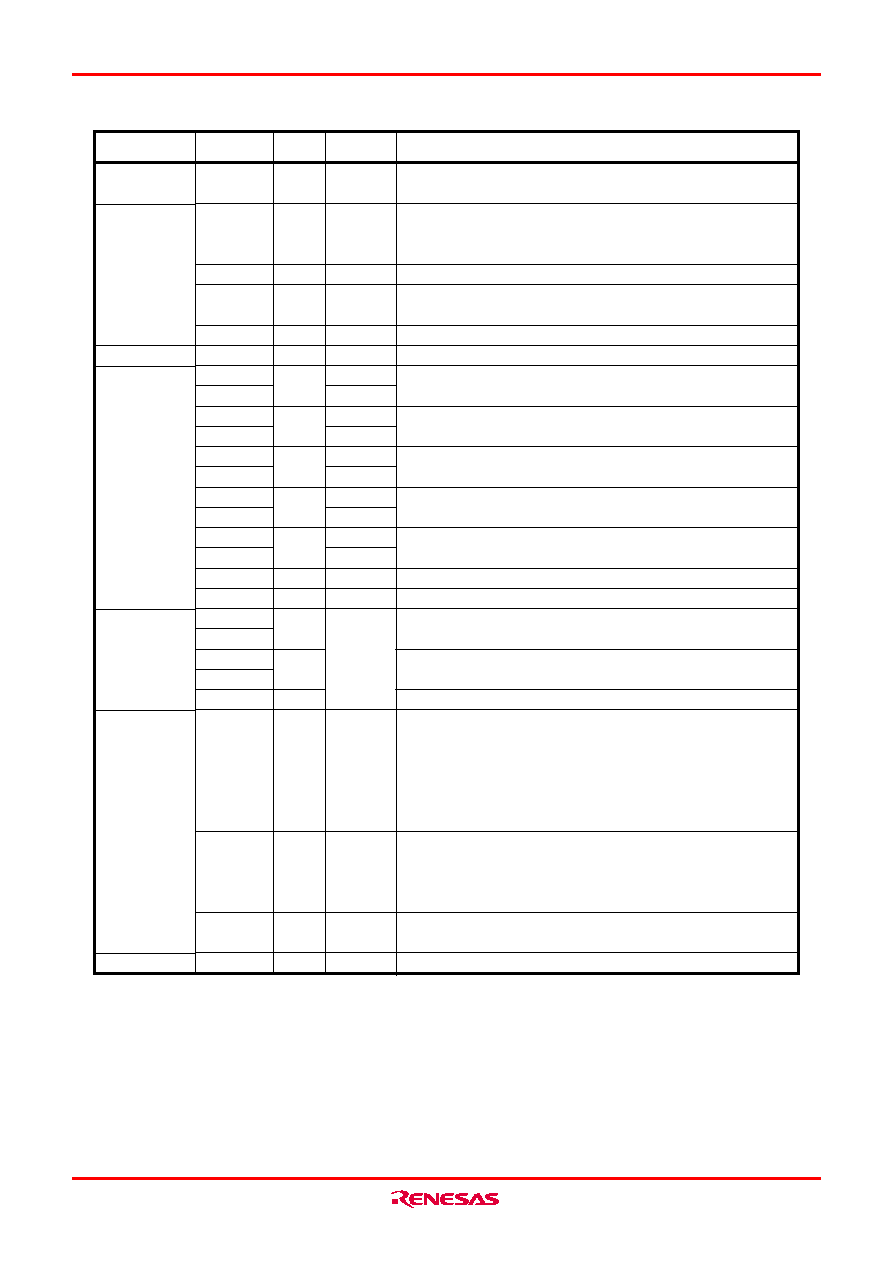
VREF
AN0 to AN7
AN00 to AN07
AN20 to AN27
___________
ADTRG
ANEX0
ANEX1
DA0, DA1
INPC10 to INPC13
INPC14 to INPC17
OUTC10 to OUTC13
OUTC14 to OUTC17
ISCLK0
ISCLK1
ISRXD0
ISRXD1
ISTXD0
ISTXD1
BE1IN
BE1OUT
CAN0IN
CAN1IN
CAN0OUT
CAN1OUT
_______________
CAN1WU
P00 to P07
P10 to P17
P20 to P27
P30 to P37
P40 to P47
P50 to P57
P60 to P67
P70 to P77
P90 to P97
P100 to P107
P80 to P84
P86, P87
P85
Reference
Voltage Input
A/D Converter
D/A Converter
Intelligent I/O
CAN
I/O Ports
Input Port
-
VCC1
VCC1/VCC2(1)
VCC1
VCC1/VCC2(1)
VCC1
VCC1/VCC2(1)
VCC1
VCC1/VCC2(1)
VCC1
VCC1/VCC2(1)
VCC1
VCC2
VCC1
Applies reference voltage to the A/D converter and D/A converter
Analog input pins for the A/D converter
Input pin for an external A/D trigger
Extended analog input pin for the A/D converter and output pin in
external op-amp connection mode
Extended analog input pin for the A/D converter
Output pin for the D/A converter
Input pins for the time measurement function
Output pins for the waveform generating function
(OUTC16 and OUTC17 assigned to P70 and P71 are pins for the N-channel open drain output.)
Inputs and outputs the clock for the intelligent I/O communication
function
Inputs data for the intelligent I/O communication function
Outputs data for the intelligent I/O communication function
Inputs data for the intelligent I/O communication function
Outputs data for the intelligent I/O communication function
Input pin for the CAN communication function
Output pin for the CAN communication function
Input pin for the CAN1 wake-up interrupt
I/O ports for CMOS. Each port can be programmed for input or
output under the control of the direction register. An input port
can be set, by program, for a pull-up resistor available or for no
pull-up resister available in 4-bit units
I/O ports having equivalent functions to P0
(P70 and P71 are ports for the N-channel open drain output.)
I/O ports having equivalent functions to P0
_______
Shares a pin with NMI. NMI input state can be got by reading P85
Supply
Classsfication
Symbol
I/O Type
Function
Voltage
I
I/O
I
O
I
O
I/O
I
O
I
O
I
O
I
I/O
I
I : Input
O : Output
I/O : Input and output
NOTES:
1. VCC2 is not available in the 100-pin package. VCC1 only available.
Table 1.6 Pin Description (100-Pin and 144-Pin Packages) (Continued)
相關(guān)PDF資料 |
PDF描述 |
|---|---|
| M30853FHTGP | 32-BIT, FLASH, 32 MHz, MICROCONTROLLER, PQFP100 |
| M30853MW-XXXGP | 32-BIT, MROM, 32 MHz, MICROCONTROLLER, PQFP100 |
| M30855FJGP | 32-BIT, FLASH, 32 MHz, MICROCONTROLLER, PQFP144 |
| M30855MW-XXXGP | 32-BIT, MROM, 32 MHz, MICROCONTROLLER, PQFP144 |
| M30873MJB-XXXGP | 32-BIT, MROM, 32 MHz, MICROCONTROLLER, PQFP100 |
相關(guān)代理商/技術(shù)參數(shù) |
參數(shù)描述 |
|---|---|
| M30853MW-XXXFP | 制造商:RENESAS 制造商全稱:Renesas Technology Corp 功能描述:SINGLE-CHIP 16/32-BIT CMOS MICROCOMPUTER |
| M30853MW-XXXGP | 制造商:RENESAS 制造商全稱:Renesas Technology Corp 功能描述:SINGLE-CHIP 16/32-BIT CMOS MICROCOMPUTER |
| M30855FHGP | 制造商:RENESAS 制造商全稱:Renesas Technology Corp 功能描述:SINGLE-CHIP 16/32-BIT CMOS MICROCOMPUTER |
| M30855FHGP D3 | 制造商:Renesas Electronics Corporation 功能描述: |
| M30855FHGP#D3 | 制造商:Renesas Electronics Corporation 功能描述:MCU 16BIT R8C CISC 384KB FLASH 5V 144LQFP - Trays |
發(fā)布緊急采購,3分鐘左右您將得到回復(fù)。