- 您現(xiàn)在的位置:買(mǎi)賣(mài)IC網(wǎng) > PDF目錄45010 > M30245MC-XXXGP 16-BIT, MROM, 16 MHz, MICROCONTROLLER, PQFP100 PDF資料下載
參數(shù)資料
| 型號(hào): | M30245MC-XXXGP |
| 元件分類(lèi): | 微控制器/微處理器 |
| 英文描述: | 16-BIT, MROM, 16 MHz, MICROCONTROLLER, PQFP100 |
| 封裝: | 14 X 14 MM, 0.50 MM PITCH, PLASTIC, LQFP-100 |
| 文件頁(yè)數(shù): | 58/268頁(yè) |
| 文件大小: | 2520K |
| 代理商: | M30245MC-XXXGP |
第1頁(yè)第2頁(yè)第3頁(yè)第4頁(yè)第5頁(yè)第6頁(yè)第7頁(yè)第8頁(yè)第9頁(yè)第10頁(yè)第11頁(yè)第12頁(yè)第13頁(yè)第14頁(yè)第15頁(yè)第16頁(yè)第17頁(yè)第18頁(yè)第19頁(yè)第20頁(yè)第21頁(yè)第22頁(yè)第23頁(yè)第24頁(yè)第25頁(yè)第26頁(yè)第27頁(yè)第28頁(yè)第29頁(yè)第30頁(yè)第31頁(yè)第32頁(yè)第33頁(yè)第34頁(yè)第35頁(yè)第36頁(yè)第37頁(yè)第38頁(yè)第39頁(yè)第40頁(yè)第41頁(yè)第42頁(yè)第43頁(yè)第44頁(yè)第45頁(yè)第46頁(yè)第47頁(yè)第48頁(yè)第49頁(yè)第50頁(yè)第51頁(yè)第52頁(yè)第53頁(yè)第54頁(yè)第55頁(yè)第56頁(yè)第57頁(yè)當(dāng)前第58頁(yè)第59頁(yè)第60頁(yè)第61頁(yè)第62頁(yè)第63頁(yè)第64頁(yè)第65頁(yè)第66頁(yè)第67頁(yè)第68頁(yè)第69頁(yè)第70頁(yè)第71頁(yè)第72頁(yè)第73頁(yè)第74頁(yè)第75頁(yè)第76頁(yè)第77頁(yè)第78頁(yè)第79頁(yè)第80頁(yè)第81頁(yè)第82頁(yè)第83頁(yè)第84頁(yè)第85頁(yè)第86頁(yè)第87頁(yè)第88頁(yè)第89頁(yè)第90頁(yè)第91頁(yè)第92頁(yè)第93頁(yè)第94頁(yè)第95頁(yè)第96頁(yè)第97頁(yè)第98頁(yè)第99頁(yè)第100頁(yè)第101頁(yè)第102頁(yè)第103頁(yè)第104頁(yè)第105頁(yè)第106頁(yè)第107頁(yè)第108頁(yè)第109頁(yè)第110頁(yè)第111頁(yè)第112頁(yè)第113頁(yè)第114頁(yè)第115頁(yè)第116頁(yè)第117頁(yè)第118頁(yè)第119頁(yè)第120頁(yè)第121頁(yè)第122頁(yè)第123頁(yè)第124頁(yè)第125頁(yè)第126頁(yè)第127頁(yè)第128頁(yè)第129頁(yè)第130頁(yè)第131頁(yè)第132頁(yè)第133頁(yè)第134頁(yè)第135頁(yè)第136頁(yè)第137頁(yè)第138頁(yè)第139頁(yè)第140頁(yè)第141頁(yè)第142頁(yè)第143頁(yè)第144頁(yè)第145頁(yè)第146頁(yè)第147頁(yè)第148頁(yè)第149頁(yè)第150頁(yè)第151頁(yè)第152頁(yè)第153頁(yè)第154頁(yè)第155頁(yè)第156頁(yè)第157頁(yè)第158頁(yè)第159頁(yè)第160頁(yè)第161頁(yè)第162頁(yè)第163頁(yè)第164頁(yè)第165頁(yè)第166頁(yè)第167頁(yè)第168頁(yè)第169頁(yè)第170頁(yè)第171頁(yè)第172頁(yè)第173頁(yè)第174頁(yè)第175頁(yè)第176頁(yè)第177頁(yè)第178頁(yè)第179頁(yè)第180頁(yè)第181頁(yè)第182頁(yè)第183頁(yè)第184頁(yè)第185頁(yè)第186頁(yè)第187頁(yè)第188頁(yè)第189頁(yè)第190頁(yè)第191頁(yè)第192頁(yè)第193頁(yè)第194頁(yè)第195頁(yè)第196頁(yè)第197頁(yè)第198頁(yè)第199頁(yè)第200頁(yè)第201頁(yè)第202頁(yè)第203頁(yè)第204頁(yè)第205頁(yè)第206頁(yè)第207頁(yè)第208頁(yè)第209頁(yè)第210頁(yè)第211頁(yè)第212頁(yè)第213頁(yè)第214頁(yè)第215頁(yè)第216頁(yè)第217頁(yè)第218頁(yè)第219頁(yè)第220頁(yè)第221頁(yè)第222頁(yè)第223頁(yè)第224頁(yè)第225頁(yè)第226頁(yè)第227頁(yè)第228頁(yè)第229頁(yè)第230頁(yè)第231頁(yè)第232頁(yè)第233頁(yè)第234頁(yè)第235頁(yè)第236頁(yè)第237頁(yè)第238頁(yè)第239頁(yè)第240頁(yè)第241頁(yè)第242頁(yè)第243頁(yè)第244頁(yè)第245頁(yè)第246頁(yè)第247頁(yè)第248頁(yè)第249頁(yè)第250頁(yè)第251頁(yè)第252頁(yè)第253頁(yè)第254頁(yè)第255頁(yè)第256頁(yè)第257頁(yè)第258頁(yè)第259頁(yè)第260頁(yè)第261頁(yè)第262頁(yè)第263頁(yè)第264頁(yè)第265頁(yè)第266頁(yè)第267頁(yè)第268頁(yè)
M30245 Group
I2C Bus interface mode
Rev.2.00
Oct 16, 2006
page 148 of 264
REJ03B0005-0200
UARTi Special Mode Register 2 (UiSMR2)
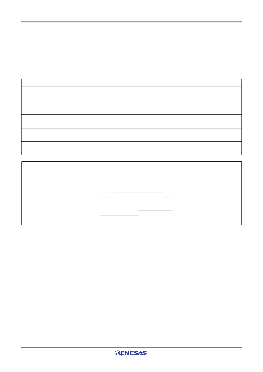
Bit 0 is the I2C mode select bit 2. Table 1.50 lists the control changes by bit when the I2C mode select bit is "1". Start
and stop condition detection timing characteristics are shown in Figure 1.107.
Table 1.50. Functions changed by I2C mode select bit 2
Function
IICM2=0
IICM2=1
Interrupt numbers 13, 15, 17, 19
factor
Acknowledge not detected (NACK)
UARTi transfer (rising edge of the
last bit)
Interrupt number 2, 8, 10, 21 factor
Acknowledge detected (ACK)
UARTi receive (falling edge of the
last bit)
DMA factor
Acknowledge detected (ACK)
UARTi receive (falling edge of the
last bit)
Data transfer timing from UART
receive shift register to receive buffer
Rising edge of the last bit of receive
clock
Rising edge of the last bit of receive
clock
UART receive/ACK interrupt request
generation timing
Rising edge of the last bit of receive
clock
Rising edge of the last bit of receive
clock
Figure 1.107. Start/stop condition detect timing characteristics
Set up time
Hold time
SCL
SDA
(Start condition)
SDA
(Stop condition)
3 to 6 cyles < set up time (Note)
3 to 6 cycles < hold time (Note)
Note: Cycle number shows main clock input oscillation frequency f(Xin) cycle number.
Bit 1 is the clock synchronizing bit. When this bit is set to "1", if the falling edge is detected at pin SCLi while the internal
SCL is "H", the internal SCL is changed to "L", the baud rate generator value is reloaded and the L sector count starts.
Also, while the SCLi pin is "L", if the internal SCL changes from "L" to "H", baud rate generator stops counting. If the SCLi
pin is "H", counting restarts. Because of this function, the UARTi transmit/receive clock takes the AND condition for the
internal SCL and SCLi pin signals. This function operates from the clock half period before the first rise of the UARTi
clock to the 9th rise. To use this function, select the internal clock as the transfer clock.
Bit 2 is the SCL wait output bit. When this bit is set to "1", output from the SCLi pin is fixed to "L" at the clock's 9th fall.
When set to "0", the "L" output lock is released. This bit is unavailable when SCLi is external clock.
Bit 3 is the SDA output stop bit. When this bit is set to "1", an arbitration lost generated. If the arbitration lost detection flag
is "1", the SDAi pin simultaneously becomes high impedance.
Bit 4 is the UARTi initialize bit. While this bit is set to "1", the following operations are performed when the start condition
is detected.
The transmit shift register is initialized and the content of the transmission register is transmitted to the transmission
shift register. Transmission starts with the first bit of the next input clock. However, the UARTi output value does not
change when the start condition is detected. It also doesn't change when the clock is input and when the first bit of data
is output.
The receive shift register is initialized and reception starts with the first bit of the next input clock.
The SCL wait output is set to "1". The SCLi pin becomes "L" level at the fall of the 9th bit of the clock.
相關(guān)PDF資料 |
PDF描述 |
|---|---|
| M30245FCGP | 16-BIT, FLASH, 16 MHz, MICROCONTROLLER, PQFP100 |
| M30260F3VGP | 16-BIT, FLASH, 20 MHz, MICROCONTROLLER, PQFP48 |
| M30260M3A-XXXGP-U5 | 16-BIT, FLASH, 20 MHz, MICROCONTROLLER, PQFP48 |
| M30260M8A-XXXGP-U5 | 16-BIT, FLASH, 20 MHz, MICROCONTROLLER, PQFP48 |
| M30263F6AFP-U7 | 16-BIT, FLASH, 20 MHz, MICROCONTROLLER, PDSO42 |
相關(guān)代理商/技術(shù)參數(shù) |
參數(shù)描述 |
|---|---|
| M30245MG | 制造商:MITSUBISHI 制造商全稱:Mitsubishi Electric Semiconductor 功能描述:SINGLE-CHIP 16-BIT CMOS MICROCOMPUTER |
| M30245MGGP | 制造商:RENESAS 制造商全稱:Renesas Technology Corp 功能描述:SINGLE-CHIP 16-BIT CMOS MICROCOMPUTER |
| M30245MG-XXXFP | 制造商:MITSUBISHI 制造商全稱:Mitsubishi Electric Semiconductor 功能描述:SINGLE-CHIP 16-BIT CMOS MICROCOMPUTER |
| M30245MG-XXXGF | 制造商:MITSUBISHI 制造商全稱:Mitsubishi Electric Semiconductor 功能描述:SINGLE-CHIP 16-BIT CMOS MICROCOMPUTER |
| M30245MG-XXXGP | 制造商:RENESAS 制造商全稱:Renesas Technology Corp 功能描述:SINGLE-CHIP 16-BIT CMOS MICROCOMPUTER |
發(fā)布緊急采購(gòu),3分鐘左右您將得到回復(fù)。