- 您現(xiàn)在的位置:買賣IC網(wǎng) > PDF目錄45010 > M30245MC-XXXGP 16-BIT, MROM, 16 MHz, MICROCONTROLLER, PQFP100 PDF資料下載
參數(shù)資料
| 型號: | M30245MC-XXXGP |
| 元件分類: | 微控制器/微處理器 |
| 英文描述: | 16-BIT, MROM, 16 MHz, MICROCONTROLLER, PQFP100 |
| 封裝: | 14 X 14 MM, 0.50 MM PITCH, PLASTIC, LQFP-100 |
| 文件頁數(shù): | 115/268頁 |
| 文件大?。?/td> | 2520K |
| 代理商: | M30245MC-XXXGP |
第1頁第2頁第3頁第4頁第5頁第6頁第7頁第8頁第9頁第10頁第11頁第12頁第13頁第14頁第15頁第16頁第17頁第18頁第19頁第20頁第21頁第22頁第23頁第24頁第25頁第26頁第27頁第28頁第29頁第30頁第31頁第32頁第33頁第34頁第35頁第36頁第37頁第38頁第39頁第40頁第41頁第42頁第43頁第44頁第45頁第46頁第47頁第48頁第49頁第50頁第51頁第52頁第53頁第54頁第55頁第56頁第57頁第58頁第59頁第60頁第61頁第62頁第63頁第64頁第65頁第66頁第67頁第68頁第69頁第70頁第71頁第72頁第73頁第74頁第75頁第76頁第77頁第78頁第79頁第80頁第81頁第82頁第83頁第84頁第85頁第86頁第87頁第88頁第89頁第90頁第91頁第92頁第93頁第94頁第95頁第96頁第97頁第98頁第99頁第100頁第101頁第102頁第103頁第104頁第105頁第106頁第107頁第108頁第109頁第110頁第111頁第112頁第113頁第114頁當前第115頁第116頁第117頁第118頁第119頁第120頁第121頁第122頁第123頁第124頁第125頁第126頁第127頁第128頁第129頁第130頁第131頁第132頁第133頁第134頁第135頁第136頁第137頁第138頁第139頁第140頁第141頁第142頁第143頁第144頁第145頁第146頁第147頁第148頁第149頁第150頁第151頁第152頁第153頁第154頁第155頁第156頁第157頁第158頁第159頁第160頁第161頁第162頁第163頁第164頁第165頁第166頁第167頁第168頁第169頁第170頁第171頁第172頁第173頁第174頁第175頁第176頁第177頁第178頁第179頁第180頁第181頁第182頁第183頁第184頁第185頁第186頁第187頁第188頁第189頁第190頁第191頁第192頁第193頁第194頁第195頁第196頁第197頁第198頁第199頁第200頁第201頁第202頁第203頁第204頁第205頁第206頁第207頁第208頁第209頁第210頁第211頁第212頁第213頁第214頁第215頁第216頁第217頁第218頁第219頁第220頁第221頁第222頁第223頁第224頁第225頁第226頁第227頁第228頁第229頁第230頁第231頁第232頁第233頁第234頁第235頁第236頁第237頁第238頁第239頁第240頁第241頁第242頁第243頁第244頁第245頁第246頁第247頁第248頁第249頁第250頁第251頁第252頁第253頁第254頁第255頁第256頁第257頁第258頁第259頁第260頁第261頁第262頁第263頁第264頁第265頁第266頁第267頁第268頁
M30245 Group
CPU Rewrite Mode
Rev.2.00
Oct 16, 2006
page 199 of 264
REJ03B0005-0200
Microcomputer Mode and Boot Mode
The control program for CPU rewrite mode must be written into the user ROM or boot ROM area in parallel I/O mode.
If the control program is written into the boot ROM area, the standard serial I/O mode becomes unusable.
Normal microcomputer mode is entered when the microcomputer is reset when pulling CNVSS pin low. In this case,
the CPU starts operating using the control program in the user ROM area.
When the microcomputer is reset by pulling the P55 pin low, and the CNVSS pin and P50 pin high, the CPU starts
operating using the control program in the boot ROM area. This mode is called the "boot" mode. The control program
in the boot ROM area can also be used to rewrite the user ROM area.
BlockAddress
Block addresses refer to the maximum even address of each block. These addresses are used in the block erase
command, lock bit program command, and read lock status command.
Software Commands
Table 1.68 lists the software commands available with the M30245 (flash memory version).
After setting the CPU rewrite mode select bit to 1, write a software command to specify an erase or program operation.
When entering a software command, the upper byte (D8 to D15) is ignored.
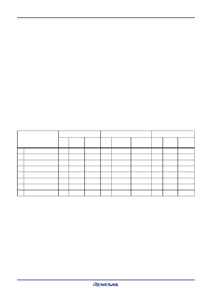
Table 1.68.
List of software commands
Note 1: When a software command is input, the data high-order byte (D8 to D15) is ignored.
Note 2: SRD= Status register data
Note 3: WA = Write address, WD = Write data.
WA and WD must be set sequentially from 0016 to FE16 (even byte address). The page size is 256 bytes.
Note 4: BA = Block address. Enter the maximum address of each block that is an even address.
Note 5: D6 corresponds to the block lock status. When D6 = "1", the unlocked blocks are "0".
Note 6: X denotes a given even address in the user ROM area.
Command
First bus cycle
Second bus cycle
Third bus cycle
Mode
Address
Data
(D0 to D7)
Mode
Address
Data
(D 0 to D7)
Mode
Address
Data
(D0 toD 7)
1
Read array
Write
X (Note 6)
FF16
2
Read status register
Write
X
7016
Read
X
SRD (Note 2)
3
Clear status register
Write
X
5016
4
Page program (Note 3)
Write
X
4116
Write
WA0 (Note 3)
WD0 (Note 3)
Write
WA1
WD1
5
Block erase
Write
X
2016
Write
BA (Note 4)
D016
6
Erase all unlocked blocks
Write
X
A716
Write
X
D016
7
Lock bit program
Write
X
7716
Write
BA
D016
8
Read lock bit status
Write
X
7116
Read
BA
D6 (Note 5)
相關(guān)PDF資料 |
PDF描述 |
|---|---|
| M30245FCGP | 16-BIT, FLASH, 16 MHz, MICROCONTROLLER, PQFP100 |
| M30260F3VGP | 16-BIT, FLASH, 20 MHz, MICROCONTROLLER, PQFP48 |
| M30260M3A-XXXGP-U5 | 16-BIT, FLASH, 20 MHz, MICROCONTROLLER, PQFP48 |
| M30260M8A-XXXGP-U5 | 16-BIT, FLASH, 20 MHz, MICROCONTROLLER, PQFP48 |
| M30263F6AFP-U7 | 16-BIT, FLASH, 20 MHz, MICROCONTROLLER, PDSO42 |
相關(guān)代理商/技術(shù)參數(shù) |
參數(shù)描述 |
|---|---|
| M30245MG | 制造商:MITSUBISHI 制造商全稱:Mitsubishi Electric Semiconductor 功能描述:SINGLE-CHIP 16-BIT CMOS MICROCOMPUTER |
| M30245MGGP | 制造商:RENESAS 制造商全稱:Renesas Technology Corp 功能描述:SINGLE-CHIP 16-BIT CMOS MICROCOMPUTER |
| M30245MG-XXXFP | 制造商:MITSUBISHI 制造商全稱:Mitsubishi Electric Semiconductor 功能描述:SINGLE-CHIP 16-BIT CMOS MICROCOMPUTER |
| M30245MG-XXXGF | 制造商:MITSUBISHI 制造商全稱:Mitsubishi Electric Semiconductor 功能描述:SINGLE-CHIP 16-BIT CMOS MICROCOMPUTER |
| M30245MG-XXXGP | 制造商:RENESAS 制造商全稱:Renesas Technology Corp 功能描述:SINGLE-CHIP 16-BIT CMOS MICROCOMPUTER |
發(fā)布緊急采購,3分鐘左右您將得到回復(fù)。