- 您現(xiàn)在的位置:買賣IC網(wǎng) > PDF目錄382635 > TMS0320F2810PBKAEP (Texas Instruments, Inc.) Digital Signal Processors PDF資料下載
參數(shù)資料
| 型號: | TMS0320F2810PBKAEP |
| 廠商: | Texas Instruments, Inc. |
| 元件分類: | 數(shù)字信號處理 |
| 英文描述: | Digital Signal Processors |
| 中文描述: | 數(shù)字信號處理器 |
| 文件頁數(shù): | 118/159頁 |
| 文件大?。?/td> | 2084K |
| 代理商: | TMS0320F2810PBKAEP |
第1頁第2頁第3頁第4頁第5頁第6頁第7頁第8頁第9頁第10頁第11頁第12頁第13頁第14頁第15頁第16頁第17頁第18頁第19頁第20頁第21頁第22頁第23頁第24頁第25頁第26頁第27頁第28頁第29頁第30頁第31頁第32頁第33頁第34頁第35頁第36頁第37頁第38頁第39頁第40頁第41頁第42頁第43頁第44頁第45頁第46頁第47頁第48頁第49頁第50頁第51頁第52頁第53頁第54頁第55頁第56頁第57頁第58頁第59頁第60頁第61頁第62頁第63頁第64頁第65頁第66頁第67頁第68頁第69頁第70頁第71頁第72頁第73頁第74頁第75頁第76頁第77頁第78頁第79頁第80頁第81頁第82頁第83頁第84頁第85頁第86頁第87頁第88頁第89頁第90頁第91頁第92頁第93頁第94頁第95頁第96頁第97頁第98頁第99頁第100頁第101頁第102頁第103頁第104頁第105頁第106頁第107頁第108頁第109頁第110頁第111頁第112頁第113頁第114頁第115頁第116頁第117頁當(dāng)前第118頁第119頁第120頁第121頁第122頁第123頁第124頁第125頁第126頁第127頁第128頁第129頁第130頁第131頁第132頁第133頁第134頁第135頁第136頁第137頁第138頁第139頁第140頁第141頁第142頁第143頁第144頁第145頁第146頁第147頁第148頁第149頁第150頁第151頁第152頁第153頁第154頁第155頁第156頁第157頁第158頁第159頁
Electrical Specifications
117
March 2004 Revised October 2004
SGUS051A
6.21
SPI Slave Mode Timing
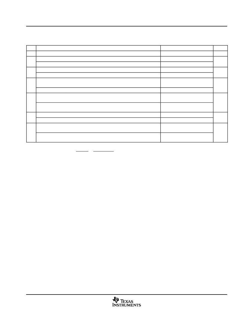
Table 623. SPI Slave Mode External Timing (Clock Phase = 0)
NO.
12
MIN
MAX
UNIT
ns
tc(SPC)S
tw(SPCH)S
tw(SPCL)S
tw(SPCL)S
tw(SPCH)S
Cycle time, SPICLK
4tc(LCO)
0.5tc(SPC)S10
0.5tc(SPC)S10
0.5tc(SPC)S10
0.5tc(SPC)S10
13§
Pulse duration, SPICLK high (clock polarity = 0)
0.5tc(SPC)S
0.5tc(SPC)S
0.5tc(SPC)S
0.5tc(SPC)S
ns
Pulse duration, SPICLK low (clock polarity = 1)
14§
Pulse duration, SPICLK low (clock polarity = 0)
ns
Pulse duration, SPICLK high (clock polarity = 1)
15§
td(SPCH-SOMI)S
Delay time, SPICLK high to SPISOMI valid
(clock polarity = 0)
0.375tc(SPC)S10
ns
td(SPCL-SOMI)S
Delay time, SPICLK low to SPISOMI valid (clock polarity = 1)
0.375tc(SPC)S10
16§
tv(SPCL-SOMI)S
Valid time, SPISOMI data valid after SPICLK low
(clock polarity =0)
0.75tc(SPC)S
ns
tv(SPCH-SOMI)S
Valid time, SPISOMI data valid after SPICLK high
(clock polarity =1)
0.75tc(SPC)S
19§
tsu(SIMO-SPCL)S
tsu(SIMO-SPCH)S
Setup time, SPISIMO before SPICLK low (clock polarity = 0)
0
ns
Setup time, SPISIMO before SPICLK high (clock polarity = 1)
0
20§
tv(SPCL-SIMO)S
Valid time, SPISIMO data valid after SPICLK low
(clock polarity = 0)
0.5tc(SPC)S
ns
tv(SPCH-SIMO)S
Valid time, SPISIMO data valid after SPICLK high
(clock polarity = 1)
0.5tc(SPC)S
The MASTER/SLAVE bit (SPICTL.2) is cleared and the CLOCK PHASE bit (SPICTL.3) is cleared.
tc(SPC) = SPI clock cycle time = LS4
(SPIBRR
tc(LCO) = LSPCLK cycle time
§The active edge of the SPICLK signal referenced is controlled by the CLOCK POLARITY bit (SPICCR.6).
or
LSPCLK
1)
相關(guān)PDF資料 |
PDF描述 |
|---|---|
| TMS20F2810PBKAEP | Digital Signal Processors |
| TMP20F2810PBKAEP | Digital Signal Processors |
| TMS320F2812PGFMEP | Digital Signal Processors |
| TMS320F2810PGFAEP | Digital Signal Processors |
| TMX20F2810PBKAEP | Digital Signal Processors |
相關(guān)代理商/技術(shù)參數(shù) |
參數(shù)描述 |
|---|---|
| TMS06105 | 制造商:Traco Power 功能描述:TMS PCB mount SMPSU,5V 6W |
| TMS06112 | 制造商:Traco Power 功能描述:TMS PCB mount SMPSU,12V 6W |
| TMS06115 | 制造商:Traco Power 功能描述:TMS PCB mount SMPSU,15V 6W |
| TMS06124 | 制造商:Traco Power 功能描述:TMS PCB mount SMPSU,24V 6W |
| TMS06212 | 制造商:Traco Power 功能描述:TMS PCB mount SMPSU,+/-12V 6W |
發(fā)布緊急采購,3分鐘左右您將得到回復(fù)。