- 您現(xiàn)在的位置:買(mǎi)賣(mài)IC網(wǎng) > PDF目錄98142 > SSTE32882HLBBKG (INTEGRATED DEVICE TECHNOLOGY INC) SSTE SERIES, PLL BASED CLOCK DRIVER, 4 TRUE OUTPUT(S), 0 INVERTED OUTPUT(S), PBGA176 PDF資料下載
參數(shù)資料
| 型號(hào): | SSTE32882HLBBKG |
| 廠商: | INTEGRATED DEVICE TECHNOLOGY INC |
| 元件分類(lèi): | 時(shí)鐘及定時(shí) |
| 英文描述: | SSTE SERIES, PLL BASED CLOCK DRIVER, 4 TRUE OUTPUT(S), 0 INVERTED OUTPUT(S), PBGA176 |
| 封裝: | 8 X 13.50 MM, 0.65 MM PITCH, GREEN, MO-246F, CABGA-176 |
| 文件頁(yè)數(shù): | 28/69頁(yè) |
| 文件大小: | 1263K |
| 代理商: | SSTE32882HLBBKG |
第1頁(yè)第2頁(yè)第3頁(yè)第4頁(yè)第5頁(yè)第6頁(yè)第7頁(yè)第8頁(yè)第9頁(yè)第10頁(yè)第11頁(yè)第12頁(yè)第13頁(yè)第14頁(yè)第15頁(yè)第16頁(yè)第17頁(yè)第18頁(yè)第19頁(yè)第20頁(yè)第21頁(yè)第22頁(yè)第23頁(yè)第24頁(yè)第25頁(yè)第26頁(yè)第27頁(yè)當(dāng)前第28頁(yè)第29頁(yè)第30頁(yè)第31頁(yè)第32頁(yè)第33頁(yè)第34頁(yè)第35頁(yè)第36頁(yè)第37頁(yè)第38頁(yè)第39頁(yè)第40頁(yè)第41頁(yè)第42頁(yè)第43頁(yè)第44頁(yè)第45頁(yè)第46頁(yè)第47頁(yè)第48頁(yè)第49頁(yè)第50頁(yè)第51頁(yè)第52頁(yè)第53頁(yè)第54頁(yè)第55頁(yè)第56頁(yè)第57頁(yè)第58頁(yè)第59頁(yè)第60頁(yè)第61頁(yè)第62頁(yè)第63頁(yè)第64頁(yè)第65頁(yè)第66頁(yè)第67頁(yè)第68頁(yè)第69頁(yè)
1.25V/1.35V/1.5V REGISTERING CLOCK DRIVER WITH PARITY TEST AND QUAD CHIP SELECT
34
SSTE32882KA1
7314/5
CONFIDENTIAL - THE INFORMATION IN THIS DOCUMENT IS SUBJECT TO CHANGE WITHOUT NOTICE
SSTE32882KA1
1.25V/1.35V/1.5V REGISTERING CLOCK DRIVER WITH PARITY TEST AND QUAD CHIP SELECT
COMMERCIAL TEMPERATURE RANGE
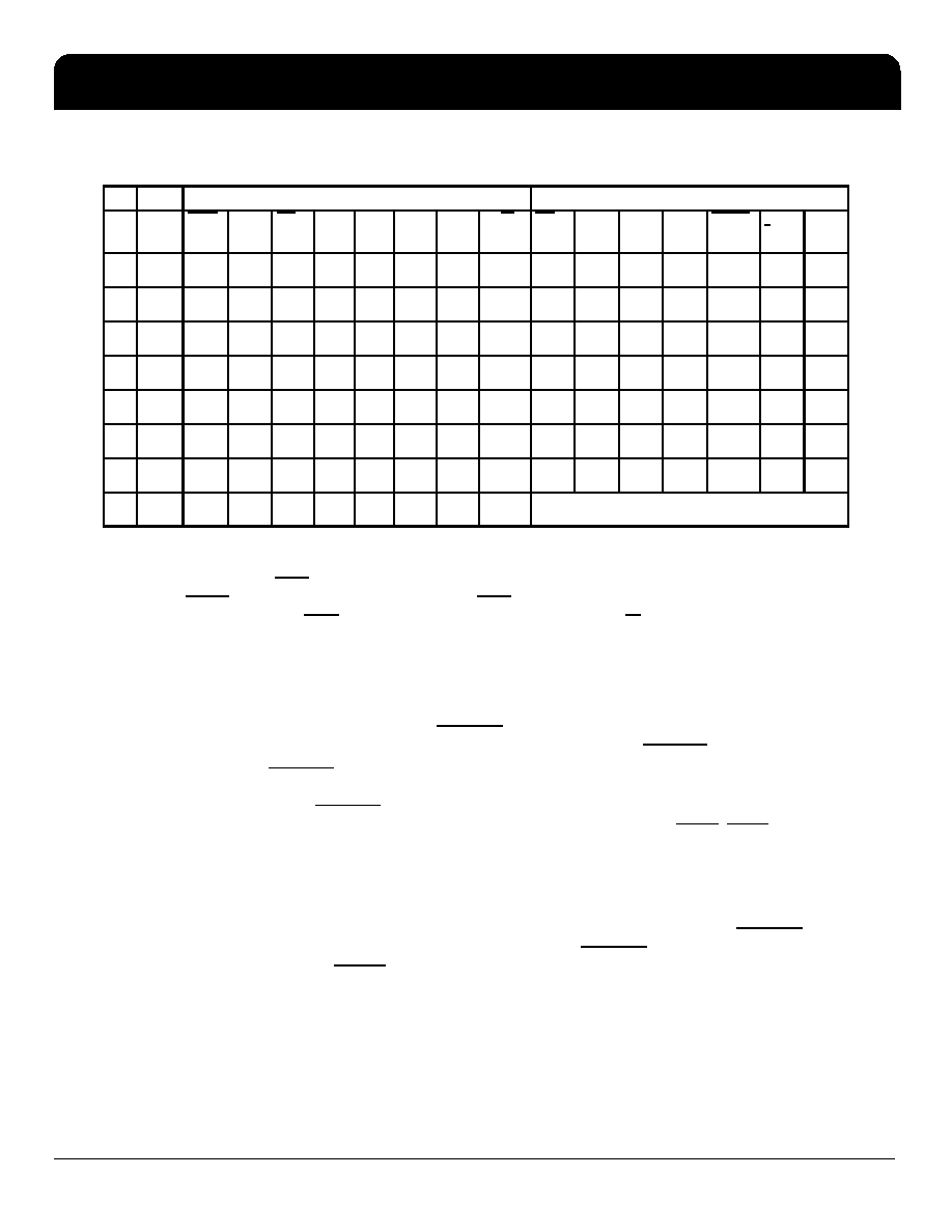
SSTE32882KA1 Device Initialization Sequence1 when Power and Clock are Stable
1. x=Logic low or lolgic high. Z=floating.
2. n = 1 for QuadCS disabled mode, n = 3 for QuadCS enabled mode.
3. The feedback clock (FBOUT and FBOUT) pins may or may not be actively driven by the device.
4. QxCKEn and ERROUT will be driven to these logic states by the register after RESET is driven low and VDD is 1.35V or 1.5V (nominal).
5. This indicates the state of QxODTx after RESET switches from low-to-high and before the rising CK edge (falling CK edge). After the first rising CK edge, within (tSTAB - tACT)
us, the state of QxODTx is a function of DODTx (high or low)
Parity
The SSTE32882KA1 includes a parity checking function. The SSTE32882KA1 accepts a parity bit from the memory
controller at its input pin PAR_IN one cycle after the corresponding data input, compares it with the data received
on the D-inputs and indicates on its open-drain ERROUT pin (active low) whether a parity error has occurred. The
computation only takes place for data which is qualified by at least one of the DCS[n:0] signals being LOW.
If an error occurs, and ERROUT is driven low with the third input clock edge after the corresponding data on the
D-inputs. It becomes high impedance with the 5th input clock cycle after the data corresponding with a parity error.
In case of consecutive errors ERROUT becomes high impedance with the 5th input clock cycle after the last data
corresponding with a parity error. The DIMM-dependent signals (DCKE0, DCKE1, DCS0, DCS1, DODT0 and
DODT1) are not included in the parity check computations.
Parity Timing Scheme Waveforms
The PAR_IN signal arrives one input clock cycle after the corresponding data input signals. ERROUT is generated
three input clock cycles after the corresponding data is registered. If ERROUTgoes low, it stays low for a minimum
of two input clock cycles or until RESET is driven low. The following figure shows the parity diagram with single
parity-error occurrence and assumes the occurrence of only one parity error when data is clocked in at the n input
clock cycle (PAR_IN clocked in on the n+1 input clock cycle).
Step Power
Inputs: Signals provided by the controller
Outputs: Signals provided by the device
VDD,
AVDD,
PVDD
RESET
Vref
DCS
[n:1]2
DODT
[0:1]
DCKE
[0:1]
DA/C
PAR_IN CK, CK
QCS
[0:1]
QODT
[0:1]
QCKE
[0:1]
QxA/C
ERROUT
Y[0:3]
FB
OUT3
0
VDD
H
stable
voltage
X
running
X
running running
1
VDD
H
stable
voltage
X
running
X
running running
2
VDD
L
stable
voltage
X
running
Z
L4
Z
H4
ZZ
3
VDD
L
stable
voltage
X
running
ZZ
LZ
HZ
Z
4
VDD
L
stable
voltage
H
X
L
X
running
Z
LZ
HZ
Z
5
VDD
L
stable
voltage
HX
L
XX
running
Z
LZ
HZ
Z
6
VDD
H
stable
voltage
HX
L
XX
running
H
L5
LX
H
running running
7
VDD
H
stable
voltage
H
X
running
After Step 6 (Step 7 and beyond), the device outputs are as defined
in the device Function Tables.
相關(guān)PDF資料 |
PDF描述 |
|---|---|
| SSTUA32864EC,557 | SSTU SERIES, POSITIVE EDGE TRIGGERED D FLIP-FLOP, TRUE OUTPUT, PBGA96 |
| SSTUA32866EC/G | 32866 SERIES, POSITIVE EDGE TRIGGERED D FLIP-FLOP, COMPLEMENTARY OUTPUT, PBGA96 |
| SSTUA32866EC,557 | 32866 SERIES, POSITIVE EDGE TRIGGERED D FLIP-FLOP, COMPLEMENTARY OUTPUT, PBGA96 |
| SSTUA32866EC/G,551 | 32866 SERIES, POSITIVE EDGE TRIGGERED D FLIP-FLOP, COMPLEMENTARY OUTPUT, PBGA96 |
| SSTUA32866EC/G,557 | 32866 SERIES, POSITIVE EDGE TRIGGERED D FLIP-FLOP, COMPLEMENTARY OUTPUT, PBGA96 |
相關(guān)代理商/技術(shù)參數(shù) |
參數(shù)描述 |
|---|---|
| SSTE32882HLBBKG8 | 制造商:Integrated Device Technology Inc 功能描述:Registering Clock Driver 176-Pin CABGA T/R 制造商:Integrated Device Technology Inc 功能描述:176 BGA (GREEN) - Tape and Reel 制造商:Integrated Device Technology Inc 功能描述:DDR3 LV REGISTER |
| SSTE32882KA1AKG | 功能描述:寄存器 RoHS:否 制造商:NXP Semiconductors 邏輯類(lèi)型:CMOS 邏輯系列:HC 電路數(shù)量:1 最大時(shí)鐘頻率:36 MHz 傳播延遲時(shí)間: 高電平輸出電流:- 7.8 mA 低電平輸出電流:7.8 mA 電源電壓-最大:6 V 最大工作溫度:+ 125 C 封裝 / 箱體:SOT-38 封裝:Tube |
| SSTE32882KA1AKG8 | 功能描述:寄存器 RoHS:否 制造商:NXP Semiconductors 邏輯類(lèi)型:CMOS 邏輯系列:HC 電路數(shù)量:1 最大時(shí)鐘頻率:36 MHz 傳播延遲時(shí)間: 高電平輸出電流:- 7.8 mA 低電平輸出電流:7.8 mA 電源電壓-最大:6 V 最大工作溫度:+ 125 C 封裝 / 箱體:SOT-38 封裝:Tube |
| SSTE32882KA1AKG8/M | 制造商:Integrated Device Technology Inc 功能描述:DDR3 REGISTER - Tape and Reel |
| SSTE32882TNA1AKG8 | 制造商:Integrated Device Technology Inc 功能描述:DDR3 REGISTER - Tape and Reel |
發(fā)布緊急采購(gòu),3分鐘左右您將得到回復(fù)。