- 您現(xiàn)在的位置:買賣IC網(wǎng) > PDF目錄299581 > ORLI10G3BM680-DB (LATTICE SEMICONDUCTOR CORP) FPGA, 1296 CLBS, 333000 GATES, PBGA680 PDF資料下載
參數(shù)資料
| 型號: | ORLI10G3BM680-DB |
| 廠商: | LATTICE SEMICONDUCTOR CORP |
| 元件分類: | FPGA |
| 英文描述: | FPGA, 1296 CLBS, 333000 GATES, PBGA680 |
| 封裝: | PLASTIC, FBGA-680 |
| 文件頁數(shù): | 44/78頁 |
| 文件大?。?/td> | 1689K |
| 代理商: | ORLI10G3BM680-DB |
第1頁第2頁第3頁第4頁第5頁第6頁第7頁第8頁第9頁第10頁第11頁第12頁第13頁第14頁第15頁第16頁第17頁第18頁第19頁第20頁第21頁第22頁第23頁第24頁第25頁第26頁第27頁第28頁第29頁第30頁第31頁第32頁第33頁第34頁第35頁第36頁第37頁第38頁第39頁第40頁第41頁第42頁第43頁當(dāng)前第44頁第45頁第46頁第47頁第48頁第49頁第50頁第51頁第52頁第53頁第54頁第55頁第56頁第57頁第58頁第59頁第60頁第61頁第62頁第63頁第64頁第65頁第66頁第67頁第68頁第69頁第70頁第71頁第72頁第73頁第74頁第75頁第76頁第77頁第78頁
Lattice Semiconductor
ORCA ORLI10G Data Sheet
49
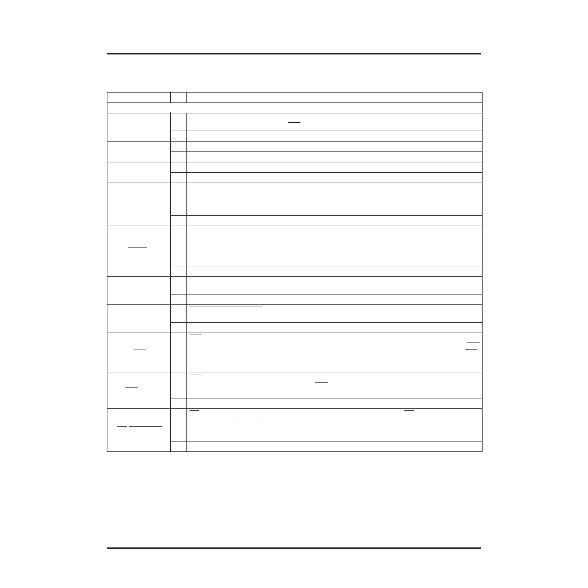
Pin Information (continued)
Table 15. Pin Descriptions (continued)
Symbol
I/O
Description
Special-Purpose Pins
M[3:0]
I
During powerup and initialization, M0—M3 are used to select the conguration mode with their val-
ues latched on the rising edge of INIT. During conguration, a pull-up is enabled.
I/O After conguration, these pins are user-programmable I/O.*
PLL_CK[0:7][TC]
I
Semidedicated PLL clock pins. During conguration they are 3-stated with a pull-up.
I/O These pins are user-programmable I/O pins if not used by PLLs after conguration.
P[TBLR]CLK[1:0][T
C]
I
Pins dedicated for the primary clock. Input pins on the middle of each side with differential pairing.
I/O After conguration, these pins are user-programmable I/O, if not used for clock inputs.
TDI, TCK, TMS
I
If boundary-scan is used, these pins are test data in, test clock, and test mode select inputs. If
boundary-scan is not selected, all boundary-scan functions are inhibited once conguration is com-
plete. Even if boundary-scan is not used, either TCK or TMS must be held at logic 1 during congu-
ration. Each pin has a pull-up enabled during conguration.
I/O After conguration, these pins are user-programmable I/O if boundary scan is not used.*
RDY/BUSY/RCLK
O
During conguration in asynchronous peripheral mode, RDY/RCLK indicates another byte can be
written to the FPGA. If a read operation is done when the device is selected, the same status is also
available on D7 in asynchronous peripheral mode.
During the master parallel conguration mode, RCLK is a read output signal to an external memory.
This output is not normally used.
I/O After conguration, this pin is a user-programmable I/O pin.*
HDC
O
High during conguration is output high until conguration is complete. It is used as a control output,
indicating that conguration is not complete.
I/O After conguration, this pin is a user-programmable I/O pin.*
LDC
O
Low during conguration is output low until conguration is complete. It is used as a control output,
indicating that conguration is not complete.
I/O After conguration, this pin is a user-programmable I/O pin.*
INIT
I/O
INIT
is a bidirectional signal before and during conguration. During conguration, a pull-up is
enabled, but an external pull-up resistor is recommended. As an active-low open-drain output, INIT
is held low during power stabilization and internal clearing of memory. As an active-low input, INIT
holds the FPGA in the wait-state before the start of conguration.
After conguration, this pin is a user-programmable I/O pin.*
CS0, CS1
I
CS0
and CS1 are used in the asynchronous peripheral, slave parallel, and microprocessor congu-
ration modes. The FPGA is selected when CS0 is low and CS1 is high. During conguration, a pull-
up is enabled.
I/O After conguration, if MPI is not used, these pins are user-programmable I/O pins.*
RD/MPI_STRB
I
RD
is used in the asynchronous peripheral conguration mode. A low on RD changes D[7:3] into a
status output. WR and RD should not be used simultaneously. If they are, the write strobe overrides.
This pin is also used as the
MPI data transfer strobe. As a status indication, a high indicates ready,
and a low indicates busy.
I/O After conguration, if the
MPI is not used, this pin is a user-programmable I/O pin.*
* The timing of DONE release is controlled by one set of bit stream options, and the timing of the simultaneous release of all
other conguration pins (and the activation of all user I/Os) is controlled by a second set of options.
相關(guān)PDF資料 |
PDF描述 |
|---|---|
| ORT82G5-1BM680 | FPGA, 1296 CLBS, 380000 GATES, PBGA680 |
| ORT82G5-2BM680 | FPGA, 1296 CLBS, 380000 GATES, PBGA680 |
| ORT82G5-3BM680 | FPGA, 1296 CLBS, 380000 GATES, PBGA680 |
| OS10040280G-012 | FIBER OPTIC RECEIVER, 1290-1600nm, PANEL MOUNT, FC/APC CONNECTOR |
| OT-WBSC-Y-A-10-X-9-M-3-05-FA | FIBER OPTIC SPLITTER/COUPLER, 1X2PORT, 10.0, PANEL MOUNT, FC/APC CONNECTOR |
相關(guān)代理商/技術(shù)參數(shù) |
參數(shù)描述 |
|---|---|
| ORLI10G-3BMN680C | 功能描述:FPGA - 現(xiàn)場可編程門陣列 10368 LUT 316 I/O RoHS:否 制造商:Altera Corporation 系列:Cyclone V E 柵極數(shù)量: 邏輯塊數(shù)量:943 內(nèi)嵌式塊RAM - EBR:1956 kbit 輸入/輸出端數(shù)量:128 最大工作頻率:800 MHz 工作電源電壓:1.1 V 最大工作溫度:+ 70 C 安裝風(fēng)格:SMD/SMT 封裝 / 箱體:FBGA-256 |
| ORLI10G5-FPSC-EV | 功能描述:可編程邏輯 IC 開發(fā)工具 ORCA ORLI10G5 FPSC Eval Brd RoHS:否 制造商:Altera Corporation 產(chǎn)品:Development Kits 類型:FPGA 工具用于評估:5CEFA7F3 接口類型: 工作電源電壓: |
| ORM0200-03600 N-70 | 制造商:SMC Corporation of America 功能描述:O-RING |
| ORM120A110 | 制造商:Ssac 功能描述: |
| ORMC615-04 | 制造商:ORTRONICS 功能描述:ORTRONICS: 15FT, CAT 6 JUMPERS, YELLOW |
發(fā)布緊急采購,3分鐘左右您將得到回復(fù)。