- 您現(xiàn)在的位置:買賣IC網(wǎng) > PDF目錄384797 > OR4E10 (Lineage Power) Field-Programmable Gate Arrays(現(xiàn)場可編程門陣列) PDF資料下載
參數(shù)資料
| 型號(hào): | OR4E10 |
| 廠商: | Lineage Power |
| 英文描述: | Field-Programmable Gate Arrays(現(xiàn)場可編程門陣列) |
| 中文描述: | 現(xiàn)場可編程門陣列(現(xiàn)場可編程門陣列) |
| 文件頁數(shù): | 45/132頁 |
| 文件大小: | 2667K |
| 代理商: | OR4E10 |
第1頁第2頁第3頁第4頁第5頁第6頁第7頁第8頁第9頁第10頁第11頁第12頁第13頁第14頁第15頁第16頁第17頁第18頁第19頁第20頁第21頁第22頁第23頁第24頁第25頁第26頁第27頁第28頁第29頁第30頁第31頁第32頁第33頁第34頁第35頁第36頁第37頁第38頁第39頁第40頁第41頁第42頁第43頁第44頁當(dāng)前第45頁第46頁第47頁第48頁第49頁第50頁第51頁第52頁第53頁第54頁第55頁第56頁第57頁第58頁第59頁第60頁第61頁第62頁第63頁第64頁第65頁第66頁第67頁第68頁第69頁第70頁第71頁第72頁第73頁第74頁第75頁第76頁第77頁第78頁第79頁第80頁第81頁第82頁第83頁第84頁第85頁第86頁第87頁第88頁第89頁第90頁第91頁第92頁第93頁第94頁第95頁第96頁第97頁第98頁第99頁第100頁第101頁第102頁第103頁第104頁第105頁第106頁第107頁第108頁第109頁第110頁第111頁第112頁第113頁第114頁第115頁第116頁第117頁第118頁第119頁第120頁第121頁第122頁第123頁第124頁第125頁第126頁第127頁第128頁第129頁第130頁第131頁第132頁
Lucent Technologies Inc.
45
Preliminary Data Sheet
August 2000
ORCA Series 4 FPGAs
Special Function Blocks
(continued)
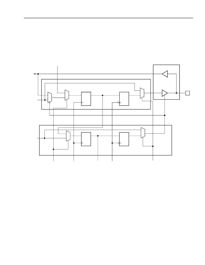
The MODE signal is generated from the decode of the instruction register. When the MODE signal is high
(EXTEST), the scan data is propagated to the output buffer. When the MODE signal is low (BYPASS or SAMPLE),
functional data from the FPGA’s internal logic is propagated to the output buffer.
The boundary-scan description language (BSDL) is provided for each device in the ORCA Series of FPGAs on the
ORCA Foundry CD. The BSDL is generated from a device profile, pinout, and other boundary-scan information.
5-2844(F)
Figure 29. Boundary-Scan Cell
Boundary-Scan Timing
To ensure race-free operation, data changes on specific clock edges. The TMS and TDI inputs are clocked in on
the rising edge of TCK, while changes on TDO occur on the falling edge of TCK. In the execution of an EXTEST
instruction, parallel data is output from the BSR to the FPGA pads on the falling edge of TCK. The maximum fre-
quency allowed for TCK is 10 MHz.
Figure 30 shows timing waveforms for an instruction scan operation. The diagram shows the use of TMS to
sequence the TAPC through states. The test host (or BSM) changes data on the falling edge of TCK, and it is
clocked into the DUT on the rising edge.
D
Q
D
Q
D
Q
D
Q
SCAN IN
p_out
HOLI
BIDIRECTIONAL DATA CELL
I/O BUFFER
DIRECTION CONTROL CELL
MODE
UPDATE/TCK
SCAN OUT
TCK
SHIFTN/CAPTURE
p_ts
p_in
PAD_IN
PAD_TS
PAD_OUT
0
1
0
1
0
1
0
1
0
1
相關(guān)PDF資料 |
PDF描述 |
|---|---|
| OR4E14 | Field-Programmable Gate Arrays(現(xiàn)場可編程門陣列) |
| OR4E2 | Field-Programmable Gate Arrays(現(xiàn)場可編程門陣列) |
| OR4E4 | Field-Programmable Gate Arrays(現(xiàn)場可編程門陣列) |
| OR4E6 | Field-Programmable Gate Arrays(現(xiàn)場可編程門陣列) |
| ORT4622 | Field-Programmable System Chip (FPSC) Four Channel x 622 Mbits/s Backplane Transceiver(現(xiàn)場可編程系統(tǒng)芯片(四通道x 622 M位/秒背板收發(fā)器)) |
相關(guān)代理商/技術(shù)參數(shù) |
參數(shù)描述 |
|---|---|
| OR4E14 | 制造商:未知廠家 制造商全稱:未知廠家 功能描述:Field-Programmable Gate Arrays |
| OR4E2 | 制造商:AGERE 制造商全稱:AGERE 功能描述:Field-Programmable Gate Arrays |
| OR4E2-1BA256 | 制造商:未知廠家 制造商全稱:未知廠家 功能描述:FPGA |
| OR4E2-1BA352 | 制造商:未知廠家 制造商全稱:未知廠家 功能描述:FPGA |
| OR4E2-1BA416 | 制造商:未知廠家 制造商全稱:未知廠家 功能描述:FPGA |
發(fā)布緊急采購,3分鐘左右您將得到回復(fù)。