- 您現(xiàn)在的位置:買賣IC網(wǎng) > PDF目錄384797 > OR4E10 (Lineage Power) Field-Programmable Gate Arrays(現(xiàn)場(chǎng)可編程門陣列) PDF資料下載
參數(shù)資料
| 型號(hào): | OR4E10 |
| 廠商: | Lineage Power |
| 英文描述: | Field-Programmable Gate Arrays(現(xiàn)場(chǎng)可編程門陣列) |
| 中文描述: | 現(xiàn)場(chǎng)可編程門陣列(現(xiàn)場(chǎng)可編程門陣列) |
| 文件頁(yè)數(shù): | 26/132頁(yè) |
| 文件大小: | 2667K |
| 代理商: | OR4E10 |
第1頁(yè)第2頁(yè)第3頁(yè)第4頁(yè)第5頁(yè)第6頁(yè)第7頁(yè)第8頁(yè)第9頁(yè)第10頁(yè)第11頁(yè)第12頁(yè)第13頁(yè)第14頁(yè)第15頁(yè)第16頁(yè)第17頁(yè)第18頁(yè)第19頁(yè)第20頁(yè)第21頁(yè)第22頁(yè)第23頁(yè)第24頁(yè)第25頁(yè)當(dāng)前第26頁(yè)第27頁(yè)第28頁(yè)第29頁(yè)第30頁(yè)第31頁(yè)第32頁(yè)第33頁(yè)第34頁(yè)第35頁(yè)第36頁(yè)第37頁(yè)第38頁(yè)第39頁(yè)第40頁(yè)第41頁(yè)第42頁(yè)第43頁(yè)第44頁(yè)第45頁(yè)第46頁(yè)第47頁(yè)第48頁(yè)第49頁(yè)第50頁(yè)第51頁(yè)第52頁(yè)第53頁(yè)第54頁(yè)第55頁(yè)第56頁(yè)第57頁(yè)第58頁(yè)第59頁(yè)第60頁(yè)第61頁(yè)第62頁(yè)第63頁(yè)第64頁(yè)第65頁(yè)第66頁(yè)第67頁(yè)第68頁(yè)第69頁(yè)第70頁(yè)第71頁(yè)第72頁(yè)第73頁(yè)第74頁(yè)第75頁(yè)第76頁(yè)第77頁(yè)第78頁(yè)第79頁(yè)第80頁(yè)第81頁(yè)第82頁(yè)第83頁(yè)第84頁(yè)第85頁(yè)第86頁(yè)第87頁(yè)第88頁(yè)第89頁(yè)第90頁(yè)第91頁(yè)第92頁(yè)第93頁(yè)第94頁(yè)第95頁(yè)第96頁(yè)第97頁(yè)第98頁(yè)第99頁(yè)第100頁(yè)第101頁(yè)第102頁(yè)第103頁(yè)第104頁(yè)第105頁(yè)第106頁(yè)第107頁(yè)第108頁(yè)第109頁(yè)第110頁(yè)第111頁(yè)第112頁(yè)第113頁(yè)第114頁(yè)第115頁(yè)第116頁(yè)第117頁(yè)第118頁(yè)第119頁(yè)第120頁(yè)第121頁(yè)第122頁(yè)第123頁(yè)第124頁(yè)第125頁(yè)第126頁(yè)第127頁(yè)第128頁(yè)第129頁(yè)第130頁(yè)第131頁(yè)第132頁(yè)
26
Lucent Technologies Inc.
Preliminary Data Sheet
August 2000
ORCA Series 4 FPGAs
Programmable Logic Cells
(continued)
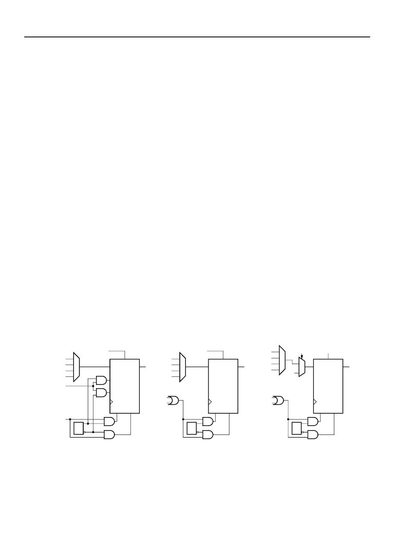
The set/reset operation of the latch/FF is controlled by
two parameters: reset mode and set/reset value. When
the GSRN and local set/reset (LSR) signals are not
asserted, the latch/FF operates normally. The reset
mode is used to select a synchronous or asynchronous
LSR operation. If synchronous, LSR has the option to
be enabled only if clock enable (CE) is active or for LSR
to have priority over the clock enable input, thereby set-
ting/resetting the FF independent of the state of the
clock enable. The clock enable is supported on FFs,
not latches. It is implemented by using a 2-input multi-
plexer on the FF input, with one input being the previ-
ous state of the FF and the other input being the new
data applied to the FF. The select of this
2-input multiplexer is clock enable (CE), which selects
either the new data or the previous state. When the
clock enable is inactive, the FF output does not change
when the clock edge arrives.
The GSRN signal is only asynchronous, and it sets/
resets all latches/FFs in the FPGA based upon the set/
reset configuration bit for each latch/FF. The set/reset
value determines whether GSRN and LSR are set or
reset inputs. The set/reset value is independent for
each latch/FF. An option is available to disable the
GSRN function per PFU after initial device configura-
tion.
The latch/FF can be configured to have a data front-
end select. Two data inputs are possible in the front-
end select mode, with the SEL signal used to select
which data input is used. The data input into each
latch/FF is from the output of its associated LUT,
F[7:0], or direct from DIN[7:0], bypassing the LUT. In
the front-end data select mode, both signals are avail-
able to the latches/FFs.
If either or both of these inputs is unused or is unavail-
able, the latch/FF data input can be tied to a logic 0 or
logic 1 instead (the default is logic 0).
The latches/FFs can be configured in three basic
modes:
I
Local synchronous set/reset: the input into the PFU’s
LSR port is used to synchronously set or reset each
latch/FF.
I
Local asynchronous set/reset: the input into LSR
asynchronously sets or resets each latch/FF.
I
Latch/FF with front-end select, LSR either synchro-
nous or asynchronous: the data select signal selects
the input into the latches/FFs between the LUT out-
put and direct data in.
For all three modes, each latch/FF can be indepen-
dently programmed as either set or reset. Figure 20
provides the logic functionality of the front-end select,
global set/reset, and local set/reset operations.
The ninth PFU FF, which is generally associated with
registering the carry-out signal in ripple mode func-
tions, can be used as a general-purpose FF. It is only
an FF and is not capable of being configured as a latch.
Because the ninth FF is not associated with an LUT,
there is no front-end data select. The data input to the
ninth FF is limited to the CIN input, logic 1, logic 0, or
the carry-out in ripple and half-logic modes.
5-9737(F).a
Key: C = configuration data.
Figure 20. Latch/FF Set/Reset Configurations
CE
CE
D
Q
S_SET
S_RESET
CLK
SET RESET
F
DIN
LOGIC 1
LOGIC 0
LSR
CD
GSRN
CE
CE
D
Q
CLK
SET RESET
F
DIN
LOGIC 1
LOGIC 0
CD
GSRN
LSR
CE
CE
D
Q
CLK
SET RESET
F
DIN
LOGIC 1
LOGIC 0
CD
GSRN
LSR
DIN
SEL
相關(guān)PDF資料 |
PDF描述 |
|---|---|
| OR4E14 | Field-Programmable Gate Arrays(現(xiàn)場(chǎng)可編程門陣列) |
| OR4E2 | Field-Programmable Gate Arrays(現(xiàn)場(chǎng)可編程門陣列) |
| OR4E4 | Field-Programmable Gate Arrays(現(xiàn)場(chǎng)可編程門陣列) |
| OR4E6 | Field-Programmable Gate Arrays(現(xiàn)場(chǎng)可編程門陣列) |
| ORT4622 | Field-Programmable System Chip (FPSC) Four Channel x 622 Mbits/s Backplane Transceiver(現(xiàn)場(chǎng)可編程系統(tǒng)芯片(四通道x 622 M位/秒背板收發(fā)器)) |
相關(guān)代理商/技術(shù)參數(shù) |
參數(shù)描述 |
|---|---|
| OR4E14 | 制造商:未知廠家 制造商全稱:未知廠家 功能描述:Field-Programmable Gate Arrays |
| OR4E2 | 制造商:AGERE 制造商全稱:AGERE 功能描述:Field-Programmable Gate Arrays |
| OR4E2-1BA256 | 制造商:未知廠家 制造商全稱:未知廠家 功能描述:FPGA |
| OR4E2-1BA352 | 制造商:未知廠家 制造商全稱:未知廠家 功能描述:FPGA |
| OR4E2-1BA416 | 制造商:未知廠家 制造商全稱:未知廠家 功能描述:FPGA |
發(fā)布緊急采購(gòu),3分鐘左右您將得到回復(fù)。