- 您現(xiàn)在的位置:買賣IC網(wǎng) > PDF目錄369923 > MPC509 (MOTOROLA INC) Highly Integrated, Low-Power, 32-Bit Microcontroller PDF資料下載
參數(shù)資料
| 型號(hào): | MPC509 |
| 廠商: | MOTOROLA INC |
| 元件分類: | 微控制器/微處理器 |
| 英文描述: | Highly Integrated, Low-Power, 32-Bit Microcontroller |
| 中文描述: | 32-BIT, RISC MICROCONTROLLER, PQFP16 |
| 文件頁數(shù): | 225/300頁 |
| 文件大小: | 3744K |
| 代理商: | MPC509 |
第1頁第2頁第3頁第4頁第5頁第6頁第7頁第8頁第9頁第10頁第11頁第12頁第13頁第14頁第15頁第16頁第17頁第18頁第19頁第20頁第21頁第22頁第23頁第24頁第25頁第26頁第27頁第28頁第29頁第30頁第31頁第32頁第33頁第34頁第35頁第36頁第37頁第38頁第39頁第40頁第41頁第42頁第43頁第44頁第45頁第46頁第47頁第48頁第49頁第50頁第51頁第52頁第53頁第54頁第55頁第56頁第57頁第58頁第59頁第60頁第61頁第62頁第63頁第64頁第65頁第66頁第67頁第68頁第69頁第70頁第71頁第72頁第73頁第74頁第75頁第76頁第77頁第78頁第79頁第80頁第81頁第82頁第83頁第84頁第85頁第86頁第87頁第88頁第89頁第90頁第91頁第92頁第93頁第94頁第95頁第96頁第97頁第98頁第99頁第100頁第101頁第102頁第103頁第104頁第105頁第106頁第107頁第108頁第109頁第110頁第111頁第112頁第113頁第114頁第115頁第116頁第117頁第118頁第119頁第120頁第121頁第122頁第123頁第124頁第125頁第126頁第127頁第128頁第129頁第130頁第131頁第132頁第133頁第134頁第135頁第136頁第137頁第138頁第139頁第140頁第141頁第142頁第143頁第144頁第145頁第146頁第147頁第148頁第149頁第150頁第151頁第152頁第153頁第154頁第155頁第156頁第157頁第158頁第159頁第160頁第161頁第162頁第163頁第164頁第165頁第166頁第167頁第168頁第169頁第170頁第171頁第172頁第173頁第174頁第175頁第176頁第177頁第178頁第179頁第180頁第181頁第182頁第183頁第184頁第185頁第186頁第187頁第188頁第189頁第190頁第191頁第192頁第193頁第194頁第195頁第196頁第197頁第198頁第199頁第200頁第201頁第202頁第203頁第204頁第205頁第206頁第207頁第208頁第209頁第210頁第211頁第212頁第213頁第214頁第215頁第216頁第217頁第218頁第219頁第220頁第221頁第222頁第223頁第224頁當(dāng)前第225頁第226頁第227頁第228頁第229頁第230頁第231頁第232頁第233頁第234頁第235頁第236頁第237頁第238頁第239頁第240頁第241頁第242頁第243頁第244頁第245頁第246頁第247頁第248頁第249頁第250頁第251頁第252頁第253頁第254頁第255頁第256頁第257頁第258頁第259頁第260頁第261頁第262頁第263頁第264頁第265頁第266頁第267頁第268頁第269頁第270頁第271頁第272頁第273頁第274頁第275頁第276頁第277頁第278頁第279頁第280頁第281頁第282頁第283頁第284頁第285頁第286頁第287頁第288頁第289頁第290頁第291頁第292頁第293頁第294頁第295頁第296頁第297頁第298頁第299頁第300頁
MPC509
USER’S MANUAL
DEVELOPMENT SUPPORT
Rev. 15 June 98
MOTOROLA
8-7
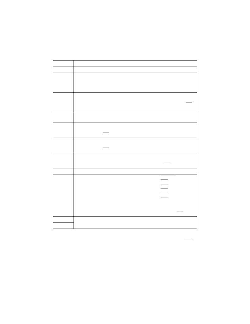
8.1.3.4 Cycle Type, Write/Read, and Address Type Pins
Cycle type pins (CT[0:3]) indicate the type of bus cycle being performed. During show
cycles, these pins are used to determine the internal address being accessed.
Table
8-6
summarizes cycle type encodings.
Notice in
Table 8-6
that during an instruction fetch (AT1 = 1) to internal memory or to
external memory resulting in a cache hit, a logic level of zero on the WR pin indicates
that the cycle is the result of an indirect change-of-flow. The indirect change-of-flow
attribute is also indicated by a cycle type encoding of 0001 when AT1 = 1. Refer to
8.1.1.1 Marking the Indirect Change-of-Flow Attribute
for additional information.
8.1.4 External Hardware During Program Trace
When program trace is needed, external hardware needs to record the status pins
(VF[0:2] and VFLS[0:1]) of each clock and record the address of all cycles marked with
the indirect change-of-flow attribute.
Table 8-6 Cycle Type Encodings
CT[0:3]
0000
Description
Normal external bus cycle
If address type is data (AT1 = 0), this is a data access to the external bus
and the start of a reservation.
If address type is instruction (AT1 = 1), this cycle type indicates that an
external address is the destination of an indirect change-of-flow.
External bus cycle to emulation memory replacing internal I-bus or L-bus
memory. An instruction access (AT1 = 1) with an address that is the target
of an indirect change-of-flow is indicated as a logic level zero on the WR
output.
Normal external bus cycle access to a port replacement chip used for
emulation support.
Access to internal I-bus memory. An instruction access (AT1 = 1) with an
address that is the target of an indirect change-of-flow is indicated as a logic
level zero on the WR output.
Access to internal L-bus memory. An instruction access (AT1 = 1) with an
address that is the target of an indirect change-of-flow is indicated as a logic
level zero on the WR output.
Cache hit on external memory address not controlled by chip selects. An
instruction access (AT1 = 1) with an address that is the target of an indirect
change-of-flow is indicated as a logic level zero on the WR output.
Access to an internal register.
Cache hit on external memory address controlled by CSBOOT.
Cache hit on external memory address controlled by CS1.
Cache hit on external memory address controlled by CS2.
Cache hit on external memory address controlled by CS3.
Cache hit on external memory address controlled by CS4.
Cache hit on external memory address controlled by CS5.
0001
0010
0011
0100
0101
0110
0111
1000
1001
1010
1011
1100
1101
An instruction access (AT1 = 1) with an address that is the target of an
indirect change-of-flow is indicated as a logic level zero on the WR output.
Reserved
1110
1111
相關(guān)PDF資料 |
PDF描述 |
|---|---|
| MPC5200BV400 | MPC5200 Hardware Specifications |
| MPC5200CBV266 | MPC5200 Hardware Specifications |
| MPC5200CBV400 | MPC5200 Hardware Specifications |
| MPC5200ID | MPC5200 Hardware Specifications |
| MPC555 | Highly Integrated, Low-Power, 32-Bit Microcontroller |
相關(guān)代理商/技術(shù)參數(shù) |
參數(shù)描述 |
|---|---|
| MPC509A | 制造商:BB 制造商全稱:BB 功能描述:Single-Ended 8-Channel/Differential 4-Channel CMOS ANALOG MULTIPLEXERS |
| MPC509AP | 功能描述:多路器開關(guān) IC 4-Ch Diff-Input Analog Mult RoHS:否 制造商:Texas Instruments 通道數(shù)量:1 開關(guān)數(shù)量:4 開啟電阻(最大值):7 Ohms 開啟時(shí)間(最大值): 關(guān)閉時(shí)間(最大值): 傳播延遲時(shí)間:0.25 ns 工作電源電壓:2.3 V to 3.6 V 工作電源電流: 最大工作溫度:+ 85 C 安裝風(fēng)格:SMD/SMT 封裝 / 箱體:UQFN-16 |
| MPC509AP | 制造商:BURR-BROWN 功能描述:IC MUX 4CH DP DIP28 509 制造商:Texas Instruments 功能描述:Multiplexer IC Multiplexer Type:Differen |
| MPC509APG4 | 功能描述:多路器開關(guān) IC 4Ch Diff-Input Ana Multiplexer RoHS:否 制造商:Texas Instruments 通道數(shù)量:1 開關(guān)數(shù)量:4 開啟電阻(最大值):7 Ohms 開啟時(shí)間(最大值): 關(guān)閉時(shí)間(最大值): 傳播延遲時(shí)間:0.25 ns 工作電源電壓:2.3 V to 3.6 V 工作電源電流: 最大工作溫度:+ 85 C 安裝風(fēng)格:SMD/SMT 封裝 / 箱體:UQFN-16 |
| MPC509AU | 功能描述:多路器開關(guān) IC 4-Ch Diff-Input Analog Mult RoHS:否 制造商:Texas Instruments 通道數(shù)量:1 開關(guān)數(shù)量:4 開啟電阻(最大值):7 Ohms 開啟時(shí)間(最大值): 關(guān)閉時(shí)間(最大值): 傳播延遲時(shí)間:0.25 ns 工作電源電壓:2.3 V to 3.6 V 工作電源電流: 最大工作溫度:+ 85 C 安裝風(fēng)格:SMD/SMT 封裝 / 箱體:UQFN-16 |
發(fā)布緊急采購,3分鐘左右您將得到回復(fù)。