- 您現(xiàn)在的位置:買賣IC網(wǎng) > PDF目錄374310 > KAB04D100M-TLGP (SAMSUNG SEMICONDUCTOR CO. LTD.) Multi-Chip Package MEMORY PDF資料下載
參數(shù)資料
| 型號(hào): | KAB04D100M-TLGP |
| 廠商: | SAMSUNG SEMICONDUCTOR CO. LTD. |
| 英文描述: | Multi-Chip Package MEMORY |
| 中文描述: | 多芯片封裝存儲(chǔ)器 |
| 文件頁數(shù): | 45/72頁 |
| 文件大小: | 1378K |
| 代理商: | KAB04D100M-TLGP |
第1頁第2頁第3頁第4頁第5頁第6頁第7頁第8頁第9頁第10頁第11頁第12頁第13頁第14頁第15頁第16頁第17頁第18頁第19頁第20頁第21頁第22頁第23頁第24頁第25頁第26頁第27頁第28頁第29頁第30頁第31頁第32頁第33頁第34頁第35頁第36頁第37頁第38頁第39頁第40頁第41頁第42頁第43頁第44頁當(dāng)前第45頁第46頁第47頁第48頁第49頁第50頁第51頁第52頁第53頁第54頁第55頁第56頁第57頁第58頁第59頁第60頁第61頁第62頁第63頁第64頁第65頁第66頁第67頁第68頁第69頁第70頁第71頁第72頁
KAB0xD100M - TxGP
Revision 1.11
August 2003
- 45 -
MCP MEMORY
SEC Only
CAPACITANCE
(T
A
= 25
°
C, V
CC
= 2.9V, f = 1.0MHz)
NOTE:
Capacitance is periodically sampled and not 100% tested.
Item
Symbol
Test Condition
Min
Max
Unit
Input Capacitance
C
IN
V
IN
=0V
-
28
pF
Input/Output Capacitance
C
IO
V
IO
=0V
-
30
pF
VALID BLOCK OF NAND FLASH MEMORY
NOTE:
1. The NAND
Flash memory
may include invalid blocks when first shipped. Additional invalid blocks may develop while being used. The number of
valid blocks is presented with both cases of invalid blocks considered. Invalid blocks are defined as blocks that contain one or more bad bits
.
Do not try to access these invalid blocks for program and erase.
Refer to the attached technical notes for a appropriate management of invalid blocks.
2. The 1st block, which is placed on 00h block address, is fully guaranteed to be a valid block, does not require Error Correction.
Parameter
Symbol
Min
Typ.
Max
Unit
Valid Block Number
N
VB
1004
-
1024
Blocks
ZZ=V
IL
CS
=V
IH
ZZ=V
IH
ZZ=V
IL
CS
U
=V
IL
, UB or/and LB=V
IL
ZZ=V
IH
CS
U
=V
IH
, ZZ=V
IH
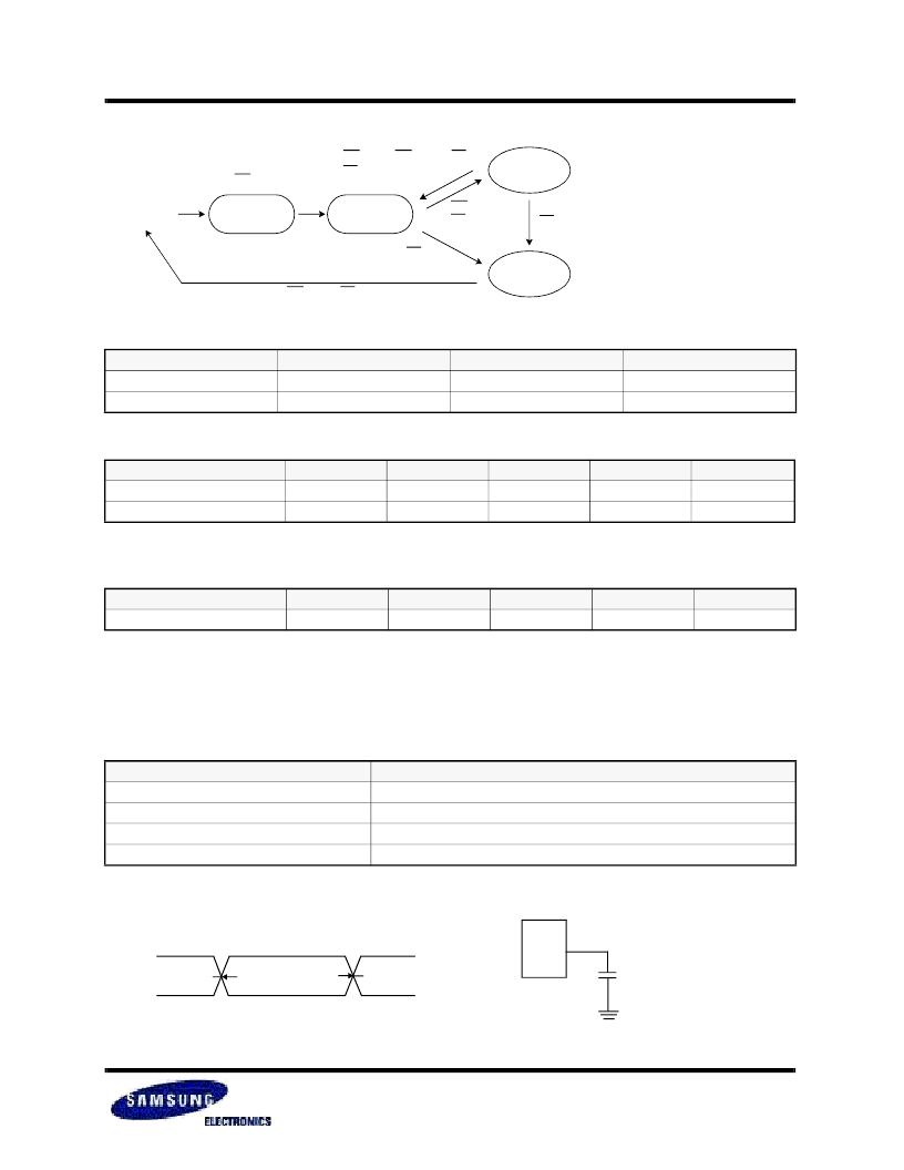
Standby Mode State Machines(U
t
RAM)
Read Operation Twice
Power On
Initial State
(Wait 200
μ
s)
Active
Standby
Mode
Deep Power
Down Mode
Standby Mode Characteristic(U
t
RAM)
Power Mode
Memory Cell Data
Standby Current(
μ
A)
Wait Time(
μ
s)
Standby
Valid
100
0
Deep Power Down
Invaild
10
200
CS
U
=V
IH
AC TEST CONDITION
NOTE:
AC test inputs are driven at Vcc
R
, Vcc
F
or Vcc
U
for a logic "1" and 0V for a logic "0". Input timing begins, and output timing ends,
at Vcc
R
/2, Vcc
F
/2 or VccQ
U
/2. Input rise and fall times (10% - 90%)<5ns. Worst case speed condition are when Vcc
R
= Vcc
R
min,
Vcc
F
= Vcc
F
min or VccQ
U
= VccQ
U
min.
Parameter
Value
Input Pulse Levels
0V to Vcc
Input Rise and Fall Times
5ns
Input and Output Timing Levels
Vcc/2 or VccQ
U
/2
C
L
= 30pF
Output Load
0V
Vcc
Vcc/2
Vcc/2 or VccQ
U
/2
Input Pulse and Test Point
Input & Output
Test Point
Output Load
*
C
L
= 30pF including Scope
and Jig Capacitance
C
L
Device
相關(guān)PDF資料 |
PDF描述 |
|---|---|
| KAB04D100M-TNGP | Multi-Chip Package MEMORY |
| KAB01D100M | Tantalum Conformal-Coated Capacitor; Capacitance: 22uF; Voltage: 10V; Packaging: Tape & Reel |
| KAB02D100M-TLGP | Tantalum Conformal-Coated Capacitor; Capacitance: 22uF; Voltage: 10V; Packaging: Tape & Reel |
| KAB01D100M-TNGP | CONNECTOR ACCESSORY |
| KAB02D100M-TNGP | CONNECTOR ACCESSORY |
相關(guān)代理商/技術(shù)參數(shù) |
參數(shù)描述 |
|---|---|
| KAB04D100M-TNGP | 制造商:SAMSUNG 制造商全稱:Samsung semiconductor 功能描述:Multi-Chip Package MEMORY |
| KAB-1 | 功能描述:保險(xiǎn)絲 TRON RECTIFIER FUSE RoHS:否 制造商:Littelfuse 產(chǎn)品:Surface Mount Fuses 電流額定值:0.5 A 電壓額定值:600 V 保險(xiǎn)絲類型:Fast Acting 保險(xiǎn)絲大小/組:Nano 尺寸:12.1 mm L x 4.5 mm W 安裝風(fēng)格: 端接類型:SMD/SMT 系列:485 |
| KAB-1/2 | 制造商:COOPER BUSSMANN 功能描述:TRON RECTIFIER FUSE |
| KAB-10 | 功能描述:保險(xiǎn)絲 10A RoHS:否 制造商:Littelfuse 產(chǎn)品:Surface Mount Fuses 電流額定值:0.5 A 電壓額定值:600 V 保險(xiǎn)絲類型:Fast Acting 保險(xiǎn)絲大小/組:Nano 尺寸:12.1 mm L x 4.5 mm W 安裝風(fēng)格: 端接類型:SMD/SMT 系列:485 |
| KAB-100 | 制造商:Cooper Bussmann 功能描述: |
發(fā)布緊急采購,3分鐘左右您將得到回復(fù)。