- 您現(xiàn)在的位置:買賣IC網(wǎng) > PDF目錄374310 > KAB01D100M-TNGP (SAMSUNG SEMICONDUCTOR CO. LTD.) CONNECTOR ACCESSORY PDF資料下載
參數(shù)資料
| 型號(hào): | KAB01D100M-TNGP |
| 廠商: | SAMSUNG SEMICONDUCTOR CO. LTD. |
| 英文描述: | CONNECTOR ACCESSORY |
| 中文描述: | 連接器附件 |
| 文件頁數(shù): | 34/72頁 |
| 文件大?。?/td> | 1378K |
| 代理商: | KAB01D100M-TNGP |
第1頁第2頁第3頁第4頁第5頁第6頁第7頁第8頁第9頁第10頁第11頁第12頁第13頁第14頁第15頁第16頁第17頁第18頁第19頁第20頁第21頁第22頁第23頁第24頁第25頁第26頁第27頁第28頁第29頁第30頁第31頁第32頁第33頁當(dāng)前第34頁第35頁第36頁第37頁第38頁第39頁第40頁第41頁第42頁第43頁第44頁第45頁第46頁第47頁第48頁第49頁第50頁第51頁第52頁第53頁第54頁第55頁第56頁第57頁第58頁第59頁第60頁第61頁第62頁第63頁第64頁第65頁第66頁第67頁第68頁第69頁第70頁第71頁第72頁
KAB0xD100M - TxGP
Revision 1.11
August 2003
- 34 -
MCP MEMORY
SEC Only
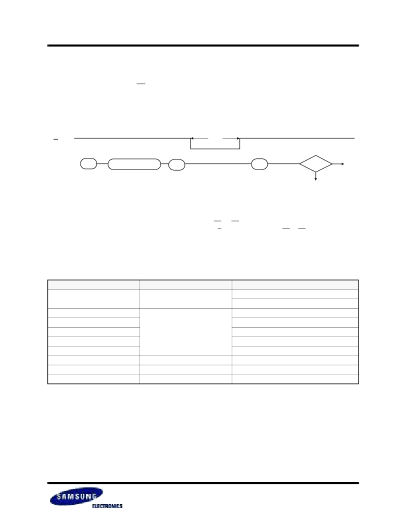
Figure 17. Block Erase Operation
BLOCK ERASE
The Erase operation is done on a block(16K Bytes) basis. Block Erase is executed by entering Erase Setup command(60h) and 2
cycle block addresses and Erase Confirm command(D0h). Only address A14 to A23 is valid while A9 to A13 is ignored. This two-
step sequence of setup followed by execution command ensures that memory contents are not accidentally erased due to external
noise condition. At the rising edge of WE after erase confirm command input, internal write controller handles erase and erase-ver-
ification. When the erase operation is completed, the Write Status Bit(I/O 0) may be checked.
Figure 6 details the sequence.
60h
Block Add. : A
9
~ A
23
DQ
x
R/B
F
Address Input(2Cycle)
DQ
0
Pass
D0h
70h
Fail
t
BERS
READ STATUS
The device contains a Status Register which may be read to find out whether program or erase operation is completed, and whether
the program or erase operation is completed successfully. After writing 70h command to command register, a read cycle takes out
the content of the Status Register to the I/O pins on the falling edge of CE
F
or RE. This two line control allows the system to poll the
progress of each device in multiple memory connections even when R/B pins are common-wired. RE or CE
F
does not need to be
toggled for updated status. Refer to table 16 for specific Status Register definitions. The command register remains in Status Read
mode until further commands are issued to it. Therefore, if the status register is read during a random read cycle, a read com-
mand(00h or 50h) should be given before sequential page read cycle.
Table 16. Read Status Register Definition
DQ #
Status
Definition
DQ
0
Program / Erase
"0" : Successful Program / Erase
"1" : Error in Program / Erase
DQ
1
Reserved for Future
Use
"0"
DQ
2
"0"
DQ
3
"0"
DQ
4
"0"
DQ
5
"0"
DQ
6
Device Operation
"0" : Busy "1" : Ready
DQ
7
Write Protect
"0" : Protected "1" : Not Protected
DQ
8~15
Not use
Don’t care
相關(guān)PDF資料 |
PDF描述 |
|---|---|
| KAB02D100M-TNGP | CONNECTOR ACCESSORY |
| KAB3403DN | White LED Step-Up Converter |
| KAB3403T | White LED Step-Up Converter |
| KAB3405T | Step Up Type DC/DC Converter for White LED |
| KAC-749S | 4-Channel power amplifier |
相關(guān)代理商/技術(shù)參數(shù) |
參數(shù)描述 |
|---|---|
| KAB02D100M-TLGP | 制造商:SAMSUNG 制造商全稱:Samsung semiconductor 功能描述:Multi-Chip Package MEMORY |
| KAB02D100M-TNGP | 制造商:SAMSUNG 制造商全稱:Samsung semiconductor 功能描述:Multi-Chip Package MEMORY |
| KAB03D100M-TLGP | 制造商:SAMSUNG 制造商全稱:Samsung semiconductor 功能描述:Multi-Chip Package MEMORY |
| KAB03D100M-TNGP | 制造商:SAMSUNG 制造商全稱:Samsung semiconductor 功能描述:Multi-Chip Package MEMORY |
| KAB04D100M-TLGP | 制造商:SAMSUNG 制造商全稱:Samsung semiconductor 功能描述:Multi-Chip Package MEMORY |
發(fā)布緊急采購,3分鐘左右您將得到回復(fù)。