- 您現(xiàn)在的位置:買賣IC網(wǎng) > PDF目錄384014 > TMC2376 (Fairchild Semiconductor Corporation) PC-to-TV Video Standards Converter(PC到TV視頻標(biāo)準(zhǔn)變換器) PDF資料下載
參數(shù)資料
| 型號(hào): | TMC2376 |
| 廠商: | Fairchild Semiconductor Corporation |
| 英文描述: | PC-to-TV Video Standards Converter(PC到TV視頻標(biāo)準(zhǔn)變換器) |
| 中文描述: | PC到電視視頻標(biāo)準(zhǔn)轉(zhuǎn)換器(電腦到電視視頻標(biāo)準(zhǔn)變換器) |
| 文件頁(yè)數(shù): | 33/48頁(yè) |
| 文件大小: | 233K |
| 代理商: | TMC2376 |
第1頁(yè)第2頁(yè)第3頁(yè)第4頁(yè)第5頁(yè)第6頁(yè)第7頁(yè)第8頁(yè)第9頁(yè)第10頁(yè)第11頁(yè)第12頁(yè)第13頁(yè)第14頁(yè)第15頁(yè)第16頁(yè)第17頁(yè)第18頁(yè)第19頁(yè)第20頁(yè)第21頁(yè)第22頁(yè)第23頁(yè)第24頁(yè)第25頁(yè)第26頁(yè)第27頁(yè)第28頁(yè)第29頁(yè)第30頁(yè)第31頁(yè)第32頁(yè)當(dāng)前第33頁(yè)第34頁(yè)第35頁(yè)第36頁(yè)第37頁(yè)第38頁(yè)第39頁(yè)第40頁(yè)第41頁(yè)第42頁(yè)第43頁(yè)第44頁(yè)第45頁(yè)第46頁(yè)第47頁(yè)第48頁(yè)
TMC2376
PRODUCT SPECIFICATION
33
P
Applications Information
Design Example–PC
Figure 27 is a reference schematic for the TMC2376. RGB
video signals and the vertical and horizontal sync signals are
intercepted by tapping connections to the VGA connector.
Typically, control of the TMC2376 will be through the serial
interface. S-video and CVBS outputs are fed to connector
that should be located at the board edge. Power is derived
from 5 volt analog, 3.3 digital 5 volt digital supplies. It is
recommended that the analog supply be clean of noise.
A 17.73 MHz PAL oscillator is shown with connection to the
CKNTSC input to provide the necessary internal clock.
For NTSC, this oscillator can be replaced with a 14.318
MHz oscillator. Systems needing both NTSC and PAL
should be set up with separate PAL and NTSC oscillators
connected to the CKIN_N and CKIN_P pins; or crystals with
appropriate capacitors connected between the CKIN_N and
CKOUT_N pins and CKIN_P and CKOUT_P pins.
Input impedance of the A/D converters exceeds 500K and
will not load VGA RGB lines. Shunt 47 pF capacitors and
274
series resistors form a low pass filter with 12 MHz cut-
off. Filtering the incoming video has two functions:
equalizing the intensities of vertical lines
eliminating sampling noise.
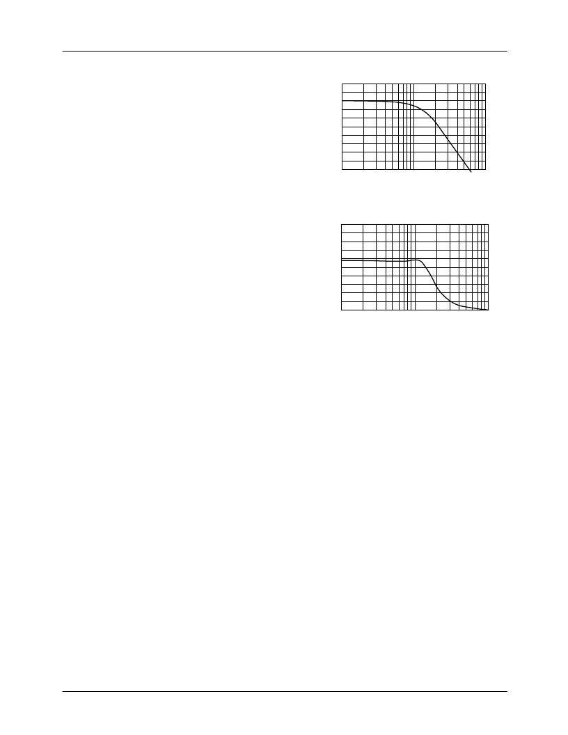
Outgoing video is filtered by low pass Bessel filters with 10
MHz cutoff. An optional low pass filter has two functions:
removal of steps from the CVBS output
limiting the bandwidth of outgoing video.
For higher definition of horizontal frequencies, a sinx/x cor-
rection filter should be incorporated to compensate for 2 dB
sampling loss of the D/A converters. Schottky diode clamps
protect the TMC2376 from high voltage transients.
Figure 25. Video Filter Response
Figure 26. Video Filter Delay
V
TIN
is derived from the bias voltage across R
REF
which is
established by the internal reference voltage available at
V
REF
. R
REF
is split into two resistors with series resistance to
set the R
REF
current and ratio to establish the V
TIN
voltage.
Design Example - TV
By interfacing the TMC2376 circuit shown in Figure 27 with
the microcontroller circuit shown in Figure 28 is a TV refer-
ence design TV reference design can be created. With this
design, many PC VGA or MAC formats can be automatically
detected by firmware resident in the 8051 microcontroller to
enable the TMC2376 to be programmed with the correct reg-
ister values for correct scaling and centering.
Only the RGB output is needed to directly drive the CRT via
the TV video amplifiers. Separate composite sync is fed to
the TV synchronization circuits that drive the horizontal and
vertical deflection circuits. The optional 10 MHz low pass
filters at the output are not required.
10.00
0.00
-10.00
-20.00
-30.00
-40.00
1
10
Frequency (MHz)
G
100
50.00
40.00
30.00
20.00
10.00
0.00
1
10
Frequency (MHz)
D
100
相關(guān)PDF資料 |
PDF描述 |
|---|---|
| TMC2490A | Multistandard Digital Video Encoder |
| TMC2490AR2C | Multistandard Digital Video Encoder |
| TMC2490 | Digital Video Encoders(數(shù)字視頻編碼器) |
| TMC2491A | Multistandard Digital Video Encoder(多標(biāo)準(zhǔn)數(shù)字視頻編碼器) |
| TMCREOJ156KTR | Low ESR Tantalum Chip Capacitors |
相關(guān)代理商/技術(shù)參數(shù) |
參數(shù)描述 |
|---|---|
| TMC239 | 制造商:未知廠家 制造商全稱:未知廠家 功能描述:High Current Microstep Stepper Motor Driver with protection / diagnosis and SPI Interface |
| TMC239_1 | 制造商:TRINAMIC 制造商全稱:TRINAMIC 功能描述:High current microstep stepper motor driver with protection, diagnostics and SPI Interface |
| TMC239A-LA | 制造商:TRINAMIC 制造商全稱:TRINAMIC 功能描述:Microstep Driver for External MOSFETs for up to 4A |
| TMC239A-SA | 制造商:Trinamic 功能描述:MICROSTEPPING MOTOR DRIVER SO-28 制造商:Trinamic 功能描述:MICROSTEPPING MOTOR DRIVER, SO-28 制造商:Trinamic 功能描述:MICROSTEPPING MOTOR DRIVER, SO-28; Motor Type:Stepper; No. of Outputs:8; Output Current:50mA; Driver Case Style:SOIC; No. of Pins:28; Supply Voltage Min:3V; Supply Voltage Max:5.5V; Operating Temperature Min:-25C; Operating ;RoHS Compliant: Yes |
| TMC239-LA | 制造商:未知廠家 制造商全稱:未知廠家 功能描述:High Current Microstep Stepper Motor Driver with protection / diagnosis and SPI Interface |
發(fā)布緊急采購(gòu),3分鐘左右您將得到回復(fù)。