- 您現(xiàn)在的位置:買賣IC網(wǎng) > PDF目錄384014 > TMC2376 (Fairchild Semiconductor Corporation) PC-to-TV Video Standards Converter(PC到TV視頻標準變換器) PDF資料下載
參數(shù)資料
| 型號: | TMC2376 |
| 廠商: | Fairchild Semiconductor Corporation |
| 英文描述: | PC-to-TV Video Standards Converter(PC到TV視頻標準變換器) |
| 中文描述: | PC到電視視頻標準轉換器(電腦到電視視頻標準變換器) |
| 文件頁數(shù): | 20/48頁 |
| 文件大?。?/td> | 233K |
| 代理商: | TMC2376 |
第1頁第2頁第3頁第4頁第5頁第6頁第7頁第8頁第9頁第10頁第11頁第12頁第13頁第14頁第15頁第16頁第17頁第18頁第19頁當前第20頁第21頁第22頁第23頁第24頁第25頁第26頁第27頁第28頁第29頁第30頁第31頁第32頁第33頁第34頁第35頁第36頁第37頁第38頁第39頁第40頁第41頁第42頁第43頁第44頁第45頁第46頁第47頁第48頁
TMC2376
PRODUCT SPECIFICATION
20
P
FSCK_OUT
t
FCO,
t
FAO
2366-07
CS
RAS
CAS
WE
A[11:0]
SDRAM Interface
Within the Frame Store Controller are pixel buffers and arbi-
tration logic that allow the alternate bursts of read and write
cycles. Pixels are transferred between the TMC2376 and the
Frame Buffer in 32-pixel length bursts.
Frame store control signals are passed to the SDRAM on the
CS, RAS, CAS, WE A
11-0
lines with data on D
16-0
. Except
for initialization CS = L. Memory Access timing is based
upon a CAS latency of 3 and burst length of 8. In the burst
mode, the SDRAM auto-increments its internal address
pointer.
There are only three types of memory access:
SDRAM Mode register setup.
Burst write. (fourth CAS incorporates an auto-precharge
cycle)
Burst read. (fourth CAS incorporates an auto-precharge
cycle)
SDRAM mode register setup is initiated by either power-up
or by RESET. Within the SDRAM, there are three fields
which are setup, as shown in Figure 6.
Figure 6. SDRAM Mode register setup
BL
2-0
= 3, sets the burst length to 8; WT = 0, establishes
sequential addressing of the burst data. LT
2-0
= 3, sets the
CAS\ latency to 3. Option bits, OP
4-0
= 0, to select the Mode
Register Set operation. Timing of the mode register write
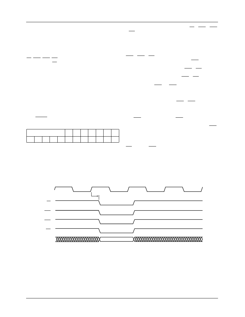
operation is shown in Figure 7. When the CS = RAS = CAS
= WE = L, the data on address bits A11-0 is stored in the
SDRAM mode register.
A 32-pixel write cycle consists of four 8-pixel burst
writes to the SDRAM. At the beginning of the write
cycle shown in Figure 8, the data bus is tri-stated with
RAS = CAS = WE = H. To start a 32-pixel burst write cycle,
a row address, ar(m) is loaded by bringing RAS = L. Three
clock cycles later, the column address ac(m) is loaded and
the first pixel d(n) written by bringing CAS = WE = L.
After pixel d(n+7) has been written, CAS = WE = L to ini-
tiate the next 8-pixel burst. After 32 pixels have been written
to the DRAM, the RAS and CAS cycles terminate and the
data bus D[15:0] is tri-stated.
During the 32-pixel burst, outgoing write addresses incre-
ment every clock cycle. Because RAS = CAS = H, the
address is ignored by the SDRAM.
Figure 10 shows a complete 32 pixel write cycle starting
with RAS = L. Next follow four CAS = L strobes while 32
pixels are stored in memory. Finally, an auto pre-charge
command is issued by address bit A10 = H for the last CAS
strobe.
A typical read cycle, as shown in Figure 9, is similar to
the write cycle. The difference is that during a read cycle,
WE = H when CAS = L. A 32-pixel read cycle will
normally be preceded by a write cycle and occasionally
be preceded by a read cycle.
OP4-0
0
LT2LT1LT0WT BL2BL1BL0
0
1
1
0
0
0
0
0
0
1
1
Figure 7. Frame Store Mode Register Write Timing
相關PDF資料 |
PDF描述 |
|---|---|
| TMC2490A | Multistandard Digital Video Encoder |
| TMC2490AR2C | Multistandard Digital Video Encoder |
| TMC2490 | Digital Video Encoders(數(shù)字視頻編碼器) |
| TMC2491A | Multistandard Digital Video Encoder(多標準數(shù)字視頻編碼器) |
| TMCREOJ156KTR | Low ESR Tantalum Chip Capacitors |
相關代理商/技術參數(shù) |
參數(shù)描述 |
|---|---|
| TMC239 | 制造商:未知廠家 制造商全稱:未知廠家 功能描述:High Current Microstep Stepper Motor Driver with protection / diagnosis and SPI Interface |
| TMC239_1 | 制造商:TRINAMIC 制造商全稱:TRINAMIC 功能描述:High current microstep stepper motor driver with protection, diagnostics and SPI Interface |
| TMC239A-LA | 制造商:TRINAMIC 制造商全稱:TRINAMIC 功能描述:Microstep Driver for External MOSFETs for up to 4A |
| TMC239A-SA | 制造商:Trinamic 功能描述:MICROSTEPPING MOTOR DRIVER SO-28 制造商:Trinamic 功能描述:MICROSTEPPING MOTOR DRIVER, SO-28 制造商:Trinamic 功能描述:MICROSTEPPING MOTOR DRIVER, SO-28; Motor Type:Stepper; No. of Outputs:8; Output Current:50mA; Driver Case Style:SOIC; No. of Pins:28; Supply Voltage Min:3V; Supply Voltage Max:5.5V; Operating Temperature Min:-25C; Operating ;RoHS Compliant: Yes |
| TMC239-LA | 制造商:未知廠家 制造商全稱:未知廠家 功能描述:High Current Microstep Stepper Motor Driver with protection / diagnosis and SPI Interface |
發(fā)布緊急采購,3分鐘左右您將得到回復。