- 您現(xiàn)在的位置:買賣IC網(wǎng) > PDF目錄384014 > TMC2376 (Fairchild Semiconductor Corporation) PC-to-TV Video Standards Converter(PC到TV視頻標(biāo)準(zhǔn)變換器) PDF資料下載
參數(shù)資料
| 型號(hào): | TMC2376 |
| 廠商: | Fairchild Semiconductor Corporation |
| 英文描述: | PC-to-TV Video Standards Converter(PC到TV視頻標(biāo)準(zhǔn)變換器) |
| 中文描述: | PC到電視視頻標(biāo)準(zhǔn)轉(zhuǎn)換器(電腦到電視視頻標(biāo)準(zhǔn)變換器) |
| 文件頁(yè)數(shù): | 26/48頁(yè) |
| 文件大?。?/td> | 233K |
| 代理商: | TMC2376 |
第1頁(yè)第2頁(yè)第3頁(yè)第4頁(yè)第5頁(yè)第6頁(yè)第7頁(yè)第8頁(yè)第9頁(yè)第10頁(yè)第11頁(yè)第12頁(yè)第13頁(yè)第14頁(yè)第15頁(yè)第16頁(yè)第17頁(yè)第18頁(yè)第19頁(yè)第20頁(yè)第21頁(yè)第22頁(yè)第23頁(yè)第24頁(yè)第25頁(yè)當(dāng)前第26頁(yè)第27頁(yè)第28頁(yè)第29頁(yè)第30頁(yè)第31頁(yè)第32頁(yè)第33頁(yè)第34頁(yè)第35頁(yè)第36頁(yè)第37頁(yè)第38頁(yè)第39頁(yè)第40頁(yè)第41頁(yè)第42頁(yè)第43頁(yè)第44頁(yè)第45頁(yè)第46頁(yè)第47頁(yè)第48頁(yè)
TMC2376
PRODUCT SPECIFICATION
26
P
There are five steps within a serial bus cycle:
1.
Start signal
2.
Slave address byte
3.
Pointer register address byte
4.
Data byte to read or write
5.
Stop signal
When the serial interface is inactive (SCL = H and SDA = H)
communications are initiated by sending a start signal. The
start signal (Figure 15, left waveform) is a HIGH-to-LOW
transition on SDA while SCL is HIGH. This signal alerts all
slaved devices that a data transfer sequence is imminent.
For 7-bit addressing, the first eight bits of data transferred
after a start signal comprise a seven bit slave address and a
single R/W bit (Read = H, Write = L). As shown in
Figure
16
, the R/W bit indicates the direction of data transfer, read
from or write to the slave device. If the transmitted slave
address matches the address of the TMC2376 (set by the
state of the SA0 and SA10/7 input pins in Table 7.), the
TMC2376 acknowledges by bringing SDA LOW on the 9th
SCL pulse (see Figure 17). If the addresses do not match, the
TMC2376 does not acknowledge.
With 10-bit addressing (see Figure 19 and Figure 19), data is
still transferred in 8-bit chunks. The upper two bits of the ten
bit address are transferred as the lower two bits of the first
byte along with the reserved sequence 11110 in the upper
five bits and the R/W bit. The lower eight bits are transferred
in the second byte without a R/W bit. Subsequent data reads
or writes follow the 7-bit transfer sequences.
For each byte of data read or written, the MSB is the first bit
of the sequence.
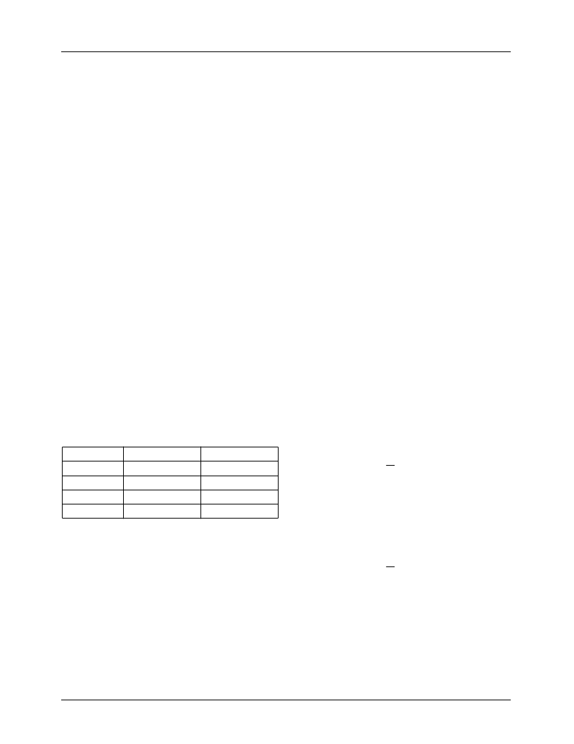
Table 7. Serial Port Addresses
Data Transfer via Serial Interface
If a slave device, such as the TMC2376 does not acknowl-
edge the master device during a write sequence, SDA
remains HIGH so the master can generate a stop signal. If
the master device does not acknowledge (ACK = L) the
TMC2376 during a read sequence, the TMC2376 interprets
this as “end of data.” SDA remains HIGH so the master can
generate a stop signal.
To write data to a specific TMC2376 control register, first the
slave address must be established by sending the slave
address byte. Next, the 8-bit pointer must be loaded with the
address of the target control register which is the base
address for subsequent write operations. Finally, the data
bytes are written, two bytes for each 10-bit register. After
each control register data transfer, the pointer address auto-
increments. If the number of bytes transferred exceeds the
number of pointer addresses, the pointer will not be incre-
mented, instead remaining at the final register value of 25
hex while an acknowledge singal, ACK is sent.
Data is read from the control registers of the TMC2376 in a
similar manner, except that two data transfer operations are
required:
1.
Write the slave address byte with bit R/W = L.
2.
Write the pointer byte.
3.
Write the slave address byte with bit R/W = H.
4.
Read the control register indexed by the pointer.
Preceding each slave write, there must be a start cycle. Fol-
lowing the pointer byte there should be a stop cycle. Sequen-
tial registers may be accessed by repeated read cycles since
pointer auto-increments after each byte transfer. After the
last read, there must be a stop cycle comprising a LOW-to-
HIGH transition of SDA while SCL is HIGH. (see
Figure
15
, right waveform)
A repeated start signal occurs when the master device driv-
ing the serial interface generates a start signal without first
generating a stop signal to terminate the current communica-
tion. This is used to change the mode of communication
(read, write) between the slave and master without releasing
the serial interface lines.
Serial Interface Read/Write Examples
Examples below show how serial bus cycles can be linked
together for multiple register read and write access cycles.
For sequential register accesses, each ACK handshake ini-
tiates further SCL clock cycles from the master to transfer
the next data byte.
Write to one 10-bit control register (two consecutive 8-bit
writes)
Start signal
Slave Address byte (R/W bit = LOW)
Pointer Address byte
Lower data byte to register
Upper data byte to register (pointer address +1)
Stop signal
Read from one 10-bit control register (two consecutive 8-bit
reads) control register
Start signal
Slave Address byte (R/W bit = LOW)
Pointer Address byte
Stop signal
Start signal
Slave Address byte (R/W bit = HIGH)
Lower data byte from pointer address
Upper byte from (pointer address + 1)
No acknowledge (terminates data transfer by
TMC2376)
SA10/7
1
1
0
0
SA0
1
0
1
0
Address (Hex)
4A
6A
224
276
相關(guān)PDF資料 |
PDF描述 |
|---|---|
| TMC2490A | Multistandard Digital Video Encoder |
| TMC2490AR2C | Multistandard Digital Video Encoder |
| TMC2490 | Digital Video Encoders(數(shù)字視頻編碼器) |
| TMC2491A | Multistandard Digital Video Encoder(多標(biāo)準(zhǔn)數(shù)字視頻編碼器) |
| TMCREOJ156KTR | Low ESR Tantalum Chip Capacitors |
相關(guān)代理商/技術(shù)參數(shù) |
參數(shù)描述 |
|---|---|
| TMC239 | 制造商:未知廠家 制造商全稱:未知廠家 功能描述:High Current Microstep Stepper Motor Driver with protection / diagnosis and SPI Interface |
| TMC239_1 | 制造商:TRINAMIC 制造商全稱:TRINAMIC 功能描述:High current microstep stepper motor driver with protection, diagnostics and SPI Interface |
| TMC239A-LA | 制造商:TRINAMIC 制造商全稱:TRINAMIC 功能描述:Microstep Driver for External MOSFETs for up to 4A |
| TMC239A-SA | 制造商:Trinamic 功能描述:MICROSTEPPING MOTOR DRIVER SO-28 制造商:Trinamic 功能描述:MICROSTEPPING MOTOR DRIVER, SO-28 制造商:Trinamic 功能描述:MICROSTEPPING MOTOR DRIVER, SO-28; Motor Type:Stepper; No. of Outputs:8; Output Current:50mA; Driver Case Style:SOIC; No. of Pins:28; Supply Voltage Min:3V; Supply Voltage Max:5.5V; Operating Temperature Min:-25C; Operating ;RoHS Compliant: Yes |
| TMC239-LA | 制造商:未知廠家 制造商全稱:未知廠家 功能描述:High Current Microstep Stepper Motor Driver with protection / diagnosis and SPI Interface |
發(fā)布緊急采購(gòu),3分鐘左右您將得到回復(fù)。