- 您現(xiàn)在的位置:買賣IC網(wǎng) > PDF目錄385819 > SC4000 (NXP SEMICONDUCTORS) Pressure Transducer, Series 19 mm, Compensated, Pressure Range: 0 psi to 200 psi, Vacuum Gage, 1/8-27 NPT, 10 Vdc excitation PDF資料下載
參數(shù)資料
| 型號(hào): | SC4000 |
| 廠商: | NXP SEMICONDUCTORS |
| 元件分類: | 路由/交換 |
| 英文描述: | Pressure Transducer, Series 19 mm, Compensated, Pressure Range: 0 psi to 200 psi, Vacuum Gage, 1/8-27 NPT, 10 Vdc excitation |
| 中文描述: | TELECOM, DIGITAL TIME SWITCH, PQFP100 |
| 封裝: | TQFP-100 |
| 文件頁(yè)數(shù): | 17/52頁(yè) |
| 文件大小: | 179K |
| 代理商: | SC4000 |
第1頁(yè)第2頁(yè)第3頁(yè)第4頁(yè)第5頁(yè)第6頁(yè)第7頁(yè)第8頁(yè)第9頁(yè)第10頁(yè)第11頁(yè)第12頁(yè)第13頁(yè)第14頁(yè)第15頁(yè)第16頁(yè)當(dāng)前第17頁(yè)第18頁(yè)第19頁(yè)第20頁(yè)第21頁(yè)第22頁(yè)第23頁(yè)第24頁(yè)第25頁(yè)第26頁(yè)第27頁(yè)第28頁(yè)第29頁(yè)第30頁(yè)第31頁(yè)第32頁(yè)第33頁(yè)第34頁(yè)第35頁(yè)第36頁(yè)第37頁(yè)第38頁(yè)第39頁(yè)第40頁(yè)第41頁(yè)第42頁(yè)第43頁(yè)第44頁(yè)第45頁(yè)第46頁(yè)第47頁(yè)第48頁(yè)第49頁(yè)第50頁(yè)第51頁(yè)第52頁(yè)
2000 Sep 07
17
Philips Semiconductors
Preliminary specification
Universal Timeslot Interchange
SC4000
CLKFAIL Timing and Control
When an SC4000 is enabled to be clock
master (C_0 = 1), the chip drives clock
and frame sync signals to the SCbus and
pulls the CLKFAIL line low. If the
SC4000 is then disabled as clock master,
the internal state machine waits for the
next frame boundary and then stops
driving clock and frame sync signals.
Instead, it drives the CLKFAIL line high
for one clock before tri-stating it (CLK-
FAIL is pulled up with 4.7K on every
board). An “armed” clock master (C_1
= 1) contains logic that monitors the
CLKFAIL line (C_51 must be set). If
CLKFAIL is sampled high for two con-
secutive clock periods, then the C_0 bit
is automatically set; the armed master
then begins driving clock and frame
sync signals and pulls CLKFAIL low.
Since the internal state machine was
using the clock and frame sync signals
driven by the previous master, the new
master takes over without any framing
error. It is as if one clock period had
been stretched, as shown in Figure 14.
Message Channel Interface
The SC4000 is designed for use with an
HDLC controller to implement the mes-
sage channel interface. The interface be-
tween an HDLC controller and SC4000
consists of the 2.048 MHz MC_CLK
(pin 11), TXD_0 (pin 9) and RXD (pin
10) lines. Data read from the SCbus MC
(pin 80) line is passed straight through
the SC4000 to the RXD output. Data
read from TXD_0 can be passed straight
through the SC4000 to the MC output,
or be buffered internally through a
clocked register. Buffering output data is
controlled by C_12. When the Message
Channel is Disabled (C_15 = 1), TXD_0
is looped back to the RXD to allow
diagnostics to be run on the HDLC
controller.
Operation Mode and Configuration
Register Setup
The SC4000 can be configured to func-
tion in five different modes shown in the
tables below:
SCbus Clock Slave (Table 1)
SCbus Clock Master (Table 2)
SCbus Armed Clock Master (Table 3)
MVIP Clock Master (Table 4)
MVIP Clock Slave (Table 5)
Table 6 shows signals that are cross
referenced by SCbus and MVIP.
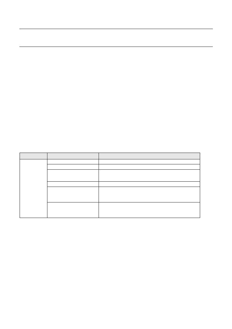
Table 1. Configuration Register Setup for SCbus Clock Slave
Operation Mode
Conguration Register Bits Setup
Function Description
SCbus Slave
C_0 = 0
SCbus clock master disabled (Default)
C_1 = 0
SCbus clock master disarmed (Default)
C_2
SCbus Primary or Alternate Select
0: Primary SCbus signals selected (Default)
1: Alternate SCbus signals selected
C_3 = 0
Diagnostic mode disabled (Note)
C_[5:4]
SCbus Framng mode to select one of the following rate:
0X = 2.048 Mb/s, 256 Bits/Frame, 32 Timeslots/Frame (Default)
10 = 4.096 Mb/s, 512 Bits/Frame, 64 Timeslots/Frame
11 = 8.192 Mb/s, 1024 Bits/Frame, 128 Timeslots/Frame
C_[7:6]
Local bus Framng mode to select one of the following rate:
0X = 2.048 Mb/s, 256 Bits/Frame, 32 Timeslots/Frame (Default)
10 = 4.096 Mb/s, 512 Bits/Frame, 64 Timeslots/Frame
11 = 8.192 Mb/s, 1024 Bits/Frame, 128 Timeslots/Frame
Note:
Default of all configuration register bits except C_3 are 0
相關(guān)PDF資料 |
PDF描述 |
|---|---|
| SC68C94 | nullQuad universal asynchronous receiver/transmitter QUART |
| SC68C94A1A | nullQuad universal asynchronous receiver/transmitter QUART |
| SC68C94A1N | Pressure Transducer, Series 19 mm, Compensated, Pressure Range: 0 psi to 50 psi, Gage, Cell with body o-ring, 10 Vdc excitation |
| SC68C94C1A | nullQuad universal asynchronous receiver/transmitter QUART |
| SC68C94C1N | Pressure Transducer, Series 19 mm, Compensated, Pressure Range: 0 psi to 50 psi, Gage, flush mount, 10 Vdc excitation |
相關(guān)代理商/技術(shù)參數(shù) |
參數(shù)描述 |
|---|---|
| SC4002A | 制造商:未知廠家 制造商全稱:未知廠家 功能描述:LCD MODULES SC4002A ( 40 CHARACTERS x 2 LINES ) |
| SC4002ALM-6 | 功能描述:AMPLIFIER TRIP UNIVERSAL INPUT D 制造商:cynergy 3 系列:SC 零件狀態(tài):在售 類型:過(guò)程感應(yīng) 跳脫狀態(tài):通電高/低 跳脫范圍:- 延遲時(shí)間:無(wú)延遲 電壓 - 電源:16 ~ 30VDC 輸出類型:繼電器 電路:SPDT(1 C 形) 不同電壓時(shí)的觸頭額定電流:3A @ 240VAC 安裝類型:DIN 軌道 工作溫度:0°C ~ 55°C 標(biāo)準(zhǔn)包裝:1 |
| SC4004 | 制造商:Ferraz Shawmut 功能描述: |
| SC4004A | 制造商:未知廠家 制造商全稱:未知廠家 功能描述:LCD MODULES 40 CHARACTERS x 4 LINES |
| SC4004B | 制造商:未知廠家 制造商全稱:未知廠家 功能描述:40 CHARACTERS x 4 LINES |
發(fā)布緊急采購(gòu),3分鐘左右您將得到回復(fù)。