- 您現在的位置:買賣IC網 > PDF目錄385819 > SC4000 (NXP SEMICONDUCTORS) Pressure Transducer, Series 19 mm, Compensated, Pressure Range: 0 psi to 200 psi, Vacuum Gage, 1/8-27 NPT, 10 Vdc excitation PDF資料下載
參數資料
| 型號: | SC4000 |
| 廠商: | NXP SEMICONDUCTORS |
| 元件分類: | 路由/交換 |
| 英文描述: | Pressure Transducer, Series 19 mm, Compensated, Pressure Range: 0 psi to 200 psi, Vacuum Gage, 1/8-27 NPT, 10 Vdc excitation |
| 中文描述: | TELECOM, DIGITAL TIME SWITCH, PQFP100 |
| 封裝: | TQFP-100 |
| 文件頁數: | 13/52頁 |
| 文件大?。?/td> | 179K |
| 代理商: | SC4000 |
第1頁第2頁第3頁第4頁第5頁第6頁第7頁第8頁第9頁第10頁第11頁第12頁當前第13頁第14頁第15頁第16頁第17頁第18頁第19頁第20頁第21頁第22頁第23頁第24頁第25頁第26頁第27頁第28頁第29頁第30頁第31頁第32頁第33頁第34頁第35頁第36頁第37頁第38頁第39頁第40頁第41頁第42頁第43頁第44頁第45頁第46頁第47頁第48頁第49頁第50頁第51頁第52頁
2000 Sep 07
13
Philips Semiconductors
Preliminary specification
Universal Timeslot Interchange
SC4000
Writing to the routing memory is syn-
chronized with SCbus timing. So rout-
ing information can be changed only on
time slot boundaries. All input data is
buffered in holding registers. The entire
holding register is transferred to the out-
put registers on a frame boundary basis.
All frame-bounded time slots incur a
one frame delay as they pass through the
switch. Switching data in this fashion
supports time slot bundling.
The SO outputs are tri-state controlled
on time slot boundaries by the Source
Routing Memory Switch Output Enable
Bit. This allows SO outputs from multi-
ple devices to be connected to a com-
mon line. The data sample position of
both the SCbus and the Local bus can be
selected for either 50% or 75% of the bit
cell.
In addition to switching local bus serial
data to and from the SCbus, the SC4000
provides a means of switching parallel
data through the microprocessor inter-
face to the SCbus. A frame boundary in-
terrupt helps control the timing of
parallel data accesses. Direct reading and
writing of parallel access register con-
tents makes for an efficient data transfer.
When using direct access, the control-
ling processor places the address of the
target channel on the address bus. In
this way, data can be read or written in a
single cycle. To avoid data corruption,
the application should not access the
channel for a time period defined as four
clocks before and four clocks after the
frame boundary.
The Source Routing Memory Local
Connect Enable mode allows the switch-
ing of any destination channel to
any source channel without SCbus
intervention. This mode accommodates
either serial or parallel data transfer.
Since data passes through the switch
twice in this mode, there is a two-frame
delay from input to output.
Diagnostic mode electrically disconnects
the SC4000 from the SCbus but allows
access through the local bus. This mode
is particularly useful for running board
diagnostics without upsetting the
SCbus. A Master Clock source is
required to run this mode.
The SC4000 pinout anticipates a future
version of the chip that includes an in-
ternal HDLC controller for the message
channel. To remain compatible with this
and other subsequent versions of the
SC4000, applications must write 0 to
all “Reserved (read only)” configuration
registers.
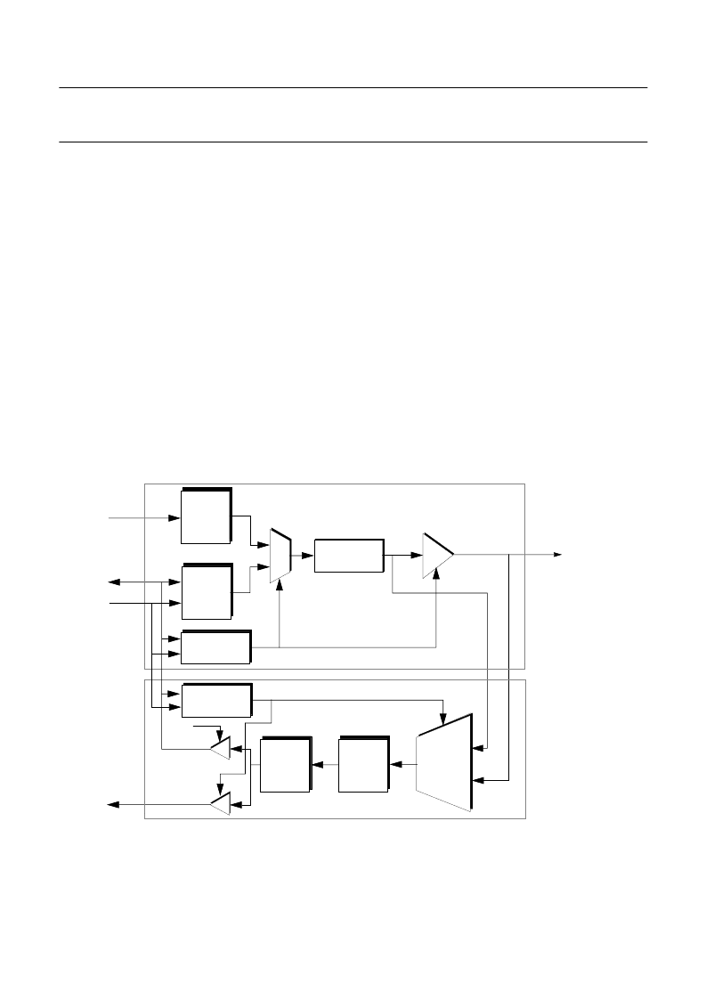
Figure 1. Destination and Source Switch Function Block
SI_[3:0]
D_[7:0]
SO_[3:0]
OUTPUT
ENABLE
READ
SOURCE
ROUTING MEMORY
DESTINATION
ROUTING MEMORY
PARALLEL
ACCESS
INPUT
HOLDING
REGISTER
PARALLEL
O
I
OUTPUT
HOLDING REGISTER
TIMESLOT & PORT
OUTPUT ENABLE
OUTPUT
HOLDING
INPUT
HOLDING
TIMESLOT,
PORT AND LOCAL
CONNECT ENABLE
1 OF 128 SOURCE SWITCH
1 OF 128 DESTINATION SWITCH
REGISTER
REGISTER
REGISTER
SD_[15:0]
L
W/R_N
相關PDF資料 |
PDF描述 |
|---|---|
| SC68C94 | nullQuad universal asynchronous receiver/transmitter QUART |
| SC68C94A1A | nullQuad universal asynchronous receiver/transmitter QUART |
| SC68C94A1N | Pressure Transducer, Series 19 mm, Compensated, Pressure Range: 0 psi to 50 psi, Gage, Cell with body o-ring, 10 Vdc excitation |
| SC68C94C1A | nullQuad universal asynchronous receiver/transmitter QUART |
| SC68C94C1N | Pressure Transducer, Series 19 mm, Compensated, Pressure Range: 0 psi to 50 psi, Gage, flush mount, 10 Vdc excitation |
相關代理商/技術參數 |
參數描述 |
|---|---|
| SC4002A | 制造商:未知廠家 制造商全稱:未知廠家 功能描述:LCD MODULES SC4002A ( 40 CHARACTERS x 2 LINES ) |
| SC4002ALM-6 | 功能描述:AMPLIFIER TRIP UNIVERSAL INPUT D 制造商:cynergy 3 系列:SC 零件狀態(tài):在售 類型:過程感應 跳脫狀態(tài):通電高/低 跳脫范圍:- 延遲時間:無延遲 電壓 - 電源:16 ~ 30VDC 輸出類型:繼電器 電路:SPDT(1 C 形) 不同電壓時的觸頭額定電流:3A @ 240VAC 安裝類型:DIN 軌道 工作溫度:0°C ~ 55°C 標準包裝:1 |
| SC4004 | 制造商:Ferraz Shawmut 功能描述: |
| SC4004A | 制造商:未知廠家 制造商全稱:未知廠家 功能描述:LCD MODULES 40 CHARACTERS x 4 LINES |
| SC4004B | 制造商:未知廠家 制造商全稱:未知廠家 功能描述:40 CHARACTERS x 4 LINES |
發(fā)布緊急采購,3分鐘左右您將得到回復。