- 您現(xiàn)在的位置:買賣IC網(wǎng) > PDF目錄98069 > S1C8F360F 8-BIT, FLASH, 8.2 MHz, MICROCONTROLLER, PQFP176 PDF資料下載
參數(shù)資料
| 型號: | S1C8F360F |
| 元件分類: | 微控制器/微處理器 |
| 英文描述: | 8-BIT, FLASH, 8.2 MHz, MICROCONTROLLER, PQFP176 |
| 封裝: | QFP18-176 |
| 文件頁數(shù): | 64/217頁 |
| 文件大小: | 1753K |
| 代理商: | S1C8F360F |
第1頁第2頁第3頁第4頁第5頁第6頁第7頁第8頁第9頁第10頁第11頁第12頁第13頁第14頁第15頁第16頁第17頁第18頁第19頁第20頁第21頁第22頁第23頁第24頁第25頁第26頁第27頁第28頁第29頁第30頁第31頁第32頁第33頁第34頁第35頁第36頁第37頁第38頁第39頁第40頁第41頁第42頁第43頁第44頁第45頁第46頁第47頁第48頁第49頁第50頁第51頁第52頁第53頁第54頁第55頁第56頁第57頁第58頁第59頁第60頁第61頁第62頁第63頁當(dāng)前第64頁第65頁第66頁第67頁第68頁第69頁第70頁第71頁第72頁第73頁第74頁第75頁第76頁第77頁第78頁第79頁第80頁第81頁第82頁第83頁第84頁第85頁第86頁第87頁第88頁第89頁第90頁第91頁第92頁第93頁第94頁第95頁第96頁第97頁第98頁第99頁第100頁第101頁第102頁第103頁第104頁第105頁第106頁第107頁第108頁第109頁第110頁第111頁第112頁第113頁第114頁第115頁第116頁第117頁第118頁第119頁第120頁第121頁第122頁第123頁第124頁第125頁第126頁第127頁第128頁第129頁第130頁第131頁第132頁第133頁第134頁第135頁第136頁第137頁第138頁第139頁第140頁第141頁第142頁第143頁第144頁第145頁第146頁第147頁第148頁第149頁第150頁第151頁第152頁第153頁第154頁第155頁第156頁第157頁第158頁第159頁第160頁第161頁第162頁第163頁第164頁第165頁第166頁第167頁第168頁第169頁第170頁第171頁第172頁第173頁第174頁第175頁第176頁第177頁第178頁第179頁第180頁第181頁第182頁第183頁第184頁第185頁第186頁第187頁第188頁第189頁第190頁第191頁第192頁第193頁第194頁第195頁第196頁第197頁第198頁第199頁第200頁第201頁第202頁第203頁第204頁第205頁第206頁第207頁第208頁第209頁第210頁第211頁第212頁第213頁第214頁第215頁第216頁第217頁
146
EPSON
S1C8F360 TECHNICAL MANUAL
7 DIFFERENCES FROM S1C883XX/S1C888XX
7 DIFFERENCES FROM S1C883XX/S1C888XX
This chapter explains the differences on functions between the S1C8F360 and the S1C883xx/888xx.
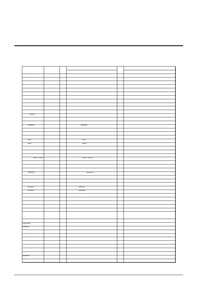
7.1 Terminal Configuration
The S1C8F360 has terminals for the PROM programmer in addition to those of the S1C883xx/888xx and
uses the QFP18-176pin or QFP21-176pin package.
Table 7.1.1 shows the pad configuration and the terminal functions according to the operating mode.
Table 7.1.1 Terminal configuration
VDD
VSS
VD1
VD1F
VOSC
VC1–VC5
CA–CE
OSC1
OSC2
OSC3
OSC4
MCU/MPU
K00–K07
K10/EVIN
K11/BREQ
R00–R07/A0–A7
R10–R17/A8–A15
R20–R22/A16–A18
R23/RD
R24/WR
R25/CL
R26/FR
R27/TOUT
R30–R33/CE0–CE3
R34/FOUT
R35–R37
R50/BZ
R51/BACK
P00–P07/D0–D7
P10/SIN
P11/SOUT
P12/SCLK
P13/SRDY
P14/CMPP0/AD4
P15/CMPM0/AD5
P16/CMPP1/AD6
P17/CMPM1/AD7
COM0–COM15
COM16–COM31
/SEG66–SEG51
SEG0–SEG50
RESET
TEST
AVDD
AVSS
AVREF
TXD
RXD
SCLK
CLKW
SPRG
VEPEXT
Pin name
Function
Normal operation mode
Serial programming mode
QFP18-176
Pin No.
86, 115
87, 156
85
66
88
82–78
77–73
89
90
83
84
93
103–96
95
94
124–131
132–139
140–142
143
144
145
146
147
148–151
152
153–155
157
158
123–116
111
110
109
108
107
106
105
104
159–174
65–50
175–176, 1–49
92
91
112
113
114
72
70
71
68
67
69
I/O
–
I
O
I
O
I
O
I/O
O
I
–
O
I
I/O
–
I
O
I
O
I
O
I
O
I
–
O
I
I/O
I
I/O
Power supply (+)
Power supply (GND)
Internal logic voltage regulator output
Internal logic and Flash voltage regulator output
Oscillation system voltage regulator output
LCD drive voltage output
Booster capacitor for LCD
OSC1 oscillation input
OSC1 oscillation output
OSC3 oscillation input
OSC3 oscillation output
MCU/MPU mode selection
Input port
Input port or EVIN input
Input port or BREQ input
Output port or address bus A0–A7
Output port or address bus A8–A15
Output port or address bus A16–A18
Output port or RD output
Output port or WR output
Output port or CL output
Output port or FR output
Output port or TOUT output
Output port or CE0–CE3 output
Output port or FOUT output
Output port
Output port or BZ output
Output port or bus BACK output
I/O port or data bus D0–D7
I/O port or SIN input
I/O port or SOUT output
I/O port or SCLK input/output
I/O port or SRDY output
I/O port, CMPP0 or AD4 input
I/O port, CMPM0 or AD5 input
I/O port, CMPP1 or AD6 input
I/O port, CMPM1 or AD7 input
LCD common output terminals
LCD common output (1/32 duty)
or LCD segment output (1/16 duty)
LCD segment output
Initial reset input
Test input
Analog power supply (+)
Analog power supply (–)
Analog reference voltage
Unused
Unused (High)
Unused
Unused (High)
N.C.
Power supply (+)
Power supply (GND)
Internal logic voltage regulator output
Internal logic and Flash voltage regulator output
Oscillation system voltage regulator output
Unused
OSC1 oscillation input
OSC1 oscillation output
Unused
Unused (High or Low)
Unused
Unused (High or Low)
Unused
Initial reset input
Unused (High)
Unused
Serial data output for Flash programming
Serial data input for Flash programming
Serial clock input/output for Flash programming
Clock input for Flash programming
Flash programming control input
Flash test (high-voltage circuit monitor)
In the parallel programming mode, all the terminals are set to the appropriate status by the exclusive
PROM writer.
相關(guān)PDF資料 |
PDF描述 |
|---|---|
| S1D13305F00B | 640 X 256 PIXELS CRT CHAR OR GRPH DSPL CTLR, PQFP60 |
| S1D13305F00A | 640 X 256 PIXELS CRT CHAR OR GRPH DSPL CTLR, PQFP60 |
| S1D13600F00A | CRT OR FLAT PNL GRPH DSPL CTLR, PQFP64 |
| S1D13700F02A100 | 320 X 240 PIXELS CRT OR FLAT PNL GRPH DSPL CTLR, PQFP64 |
| S1D13706F00A | 320 X 240 PIXELS CRT OR FLAT PNL GRPH DSPL CTLR, PQFP100 |
相關(guān)代理商/技術(shù)參數(shù) |
參數(shù)描述 |
|---|---|
| S1C8F360F413100 | 功能描述:16位微控制器 - MCU 8-bit Flash 60KB LCD Dr. 51 x 32 RoHS:否 制造商:Texas Instruments 核心:RISC 處理器系列:MSP430FR572x 數(shù)據(jù)總線寬度:16 bit 最大時鐘頻率:24 MHz 程序存儲器大小:8 KB 數(shù)據(jù) RAM 大小:1 KB 片上 ADC:Yes 工作電源電壓:2 V to 3.6 V 工作溫度范圍:- 40 C to + 85 C 封裝 / 箱體:VQFN-40 安裝風(fēng)格:SMD/SMT |
| S1C8F360F513200 | 功能描述:16位微控制器 - MCU 8-bit Flash 60KB LCD Dr. 51 x 32 RoHS:否 制造商:Texas Instruments 核心:RISC 處理器系列:MSP430FR572x 數(shù)據(jù)總線寬度:16 bit 最大時鐘頻率:24 MHz 程序存儲器大小:8 KB 數(shù)據(jù) RAM 大小:1 KB 片上 ADC:Yes 工作電源電壓:2 V to 3.6 V 工作溫度范圍:- 40 C to + 85 C 封裝 / 箱體:VQFN-40 安裝風(fēng)格:SMD/SMT |
| S1C8F626 | 制造商:EPSON 制造商全稱:EPSON 功能描述:8-bit Single Chip Microcomputer |
| S1C-8-S | 制造商:GRIPCO 功能描述: |
| S1CFB | 制造商:Hubbell Wiring Device-Kellems 功能描述:FLOORBOX, SYSTEM ONE, CAST IRON |
發(fā)布緊急采購,3分鐘左右您將得到回復(fù)。