- 您現(xiàn)在的位置:買賣IC網(wǎng) > PDF目錄98069 > S1C8F360F 8-BIT, FLASH, 8.2 MHz, MICROCONTROLLER, PQFP176 PDF資料下載
參數(shù)資料
| 型號: | S1C8F360F |
| 元件分類: | 微控制器/微處理器 |
| 英文描述: | 8-BIT, FLASH, 8.2 MHz, MICROCONTROLLER, PQFP176 |
| 封裝: | QFP18-176 |
| 文件頁數(shù): | 30/217頁 |
| 文件大?。?/td> | 1753K |
| 代理商: | S1C8F360F |
第1頁第2頁第3頁第4頁第5頁第6頁第7頁第8頁第9頁第10頁第11頁第12頁第13頁第14頁第15頁第16頁第17頁第18頁第19頁第20頁第21頁第22頁第23頁第24頁第25頁第26頁第27頁第28頁第29頁當(dāng)前第30頁第31頁第32頁第33頁第34頁第35頁第36頁第37頁第38頁第39頁第40頁第41頁第42頁第43頁第44頁第45頁第46頁第47頁第48頁第49頁第50頁第51頁第52頁第53頁第54頁第55頁第56頁第57頁第58頁第59頁第60頁第61頁第62頁第63頁第64頁第65頁第66頁第67頁第68頁第69頁第70頁第71頁第72頁第73頁第74頁第75頁第76頁第77頁第78頁第79頁第80頁第81頁第82頁第83頁第84頁第85頁第86頁第87頁第88頁第89頁第90頁第91頁第92頁第93頁第94頁第95頁第96頁第97頁第98頁第99頁第100頁第101頁第102頁第103頁第104頁第105頁第106頁第107頁第108頁第109頁第110頁第111頁第112頁第113頁第114頁第115頁第116頁第117頁第118頁第119頁第120頁第121頁第122頁第123頁第124頁第125頁第126頁第127頁第128頁第129頁第130頁第131頁第132頁第133頁第134頁第135頁第136頁第137頁第138頁第139頁第140頁第141頁第142頁第143頁第144頁第145頁第146頁第147頁第148頁第149頁第150頁第151頁第152頁第153頁第154頁第155頁第156頁第157頁第158頁第159頁第160頁第161頁第162頁第163頁第164頁第165頁第166頁第167頁第168頁第169頁第170頁第171頁第172頁第173頁第174頁第175頁第176頁第177頁第178頁第179頁第180頁第181頁第182頁第183頁第184頁第185頁第186頁第187頁第188頁第189頁第190頁第191頁第192頁第193頁第194頁第195頁第196頁第197頁第198頁第199頁第200頁第201頁第202頁第203頁第204頁第205頁第206頁第207頁第208頁第209頁第210頁第211頁第212頁第213頁第214頁第215頁第216頁第217頁
S1C8F360 TECHNICAL MANUAL
EPSON
115
5 PERIPHERAL CIRCUITS AND THEIR OPERATION (LCD Controller)
5.12.7 Display control
The display status of the built-in LCD driver and
the contrast adjustment can be controlled with the
built-in LCD controller. The LCD display status can
be selected by display control registers LCDC0 and
LCDC1. Setting the value and display status are
shown in Table 5.12.7.1.
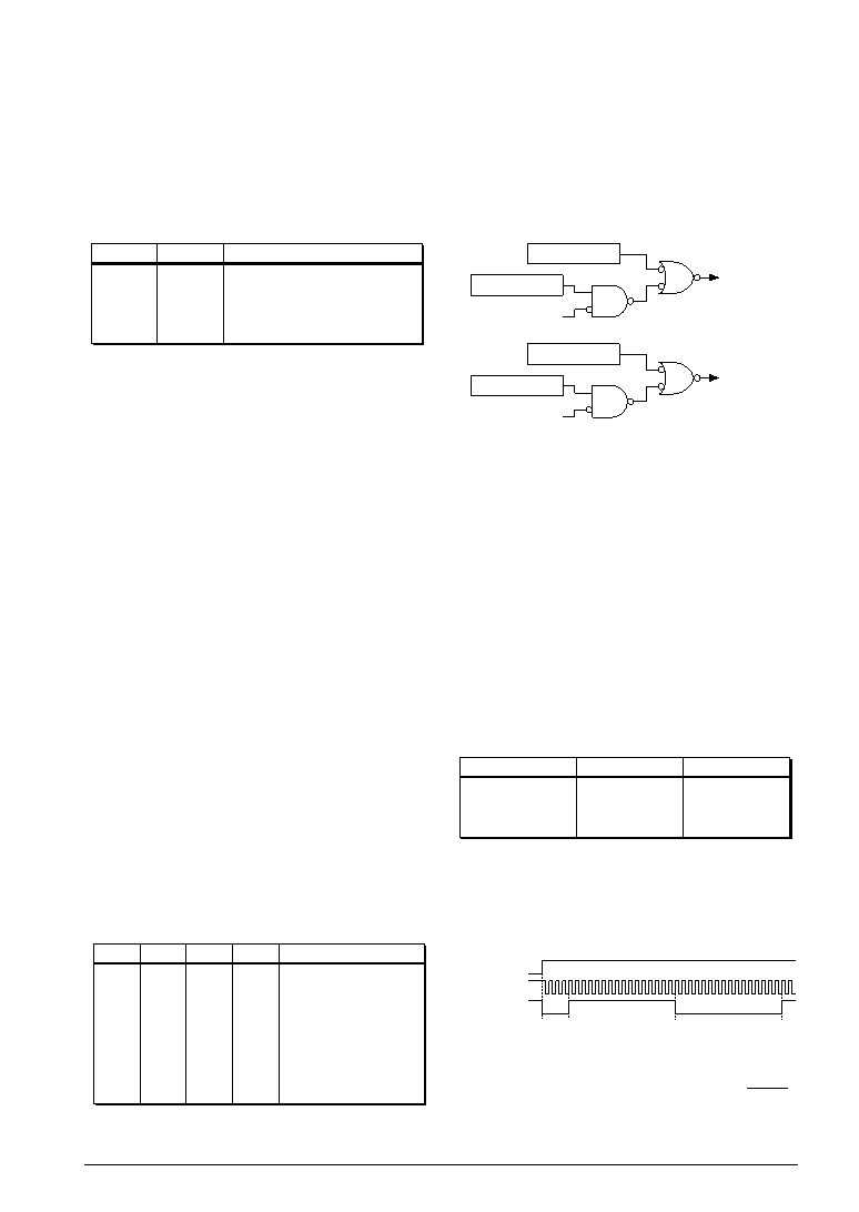
Table 5.12.7.1 LCD display control
5.12.8 CL and FR outputs
In order for the S1C8F360 to handle connection to
an externally expanded LCD driver, output ports
R25 and R26 can be used to output a CL signal
(LCD synchronous signal) and FR signal (LCD
frame signal), respectively.
The configuration of output ports R25 and R26 are
shown in Figure 5.12.8.1.
LCDC1
LCDC0
LCD display
1
0
1
0
1
0
All LCDs lit (Static)
All LCDs out (Dynamic)
Normal display
Drive OFF
All the dots in the LCD display can be turned on or
off directly by the drive waveform output from the
LCD driver, and data in the display memory is not
changed. Also, since the common terminal at this
time is set to static drive when all the dots are on
and is set to dynamic drive when they are off, this
function can be used as follows:
(1) Since all dots on is binary output (VC5 and VSS)
with static drive, the common/segment termi-
nal can be used as a monitor terminal for the
OSC1 oscillation frequency adjustment.
(2) Since all dots off is dynamic drive, you can
brink the entire LCD display without changing
display memory data.
Selecting LCD drive OFF turns the LCD drive
power circuit OFF and all the VC1–VC5 terminals go
to VSS level. However, if external power supply has
been selected by the mask option, the VC1–VC5 shift
to floating status when drive is turned OFF.
Furthermore, when the SLP instruction is executed,
registers LCDC0 and LCDC1 are automatically
reset to "0" (set to drive off) by hardware.
The LCD contrast can be adjusted in 16 stages. This
adjustment is done by the contrast adjustment
register LC0–LC3, and the setting values corre-
spond to the contrast as shown in Table 5.12.7.2.
However, if external power supply has been
selected by the mask option, the contrast adjust-
ment register LC0–LC3 is ineffective and contrast
adjustment cannot be done.
Table 5.12.7.2 LCD contrast adjustment
LC3
LC0
Contrast
1
:
0
1
0
1
:
0
1
0
Dark
Light
LC1
1
0
:
1
0
LC2
1
:
0
↑
↓
Register R25D
Register LCCLK
R25 output
CL signal
Register R26D
Register LCFRM
R26 output
FR signal
Fig. 5.12.8.1 Configuration of R25 and R26
The output control for the CL signal is done by the
register LCCLK. When you set "1" for the LCCLK,
the CL signal is output from the output port
terminal R25, when "0" is set, the HIGH (VDD) level
is output. At this time, "1" must always be set for
the data register R25D.
The output control for the FR signal is done by the
register LCFRM. When you set "1" for the LCFRM,
the FR signal is output from the output port
terminal R26, when "0" is set, the HIGH (VDD) level
is output. At this time, "1" must always be set for
the data register R26D.
The frequencies of each signal are changed as
shown in Table 5.12.8.1 according to the drive duty
selection.
Table 5.12.8.1 Frequencies of CL and FR signals
Drive duty
1/32
1/16
1/8
CL signal (Hz)
2,048
1,024
FR signal (Hz)
32
64
Since the signals are generated asynchronously
from the registers LCCLK and LCFRM, when the
signals are turned ON or OFF by the register
settings, a hazard of a 1/2 cycle or less is generated.
Figure 5.12.8.2 shows the output waveforms of the
CL and FR signals.
Fig. 5.12.8.2 Output waveforms of CL and FR signals
(when 1/16 duty is selected)
Note: The CL and FR outputs are provided for
supporting the S1C883xx. When the TOUT
output (mask option for the S1C888xx) is
selected for R26, the CL and FR signals
cannot be output.
LCCLK/LCFRM
CL output (R25)
FR output (R26)
01
相關(guān)PDF資料 |
PDF描述 |
|---|---|
| S1D13305F00B | 640 X 256 PIXELS CRT CHAR OR GRPH DSPL CTLR, PQFP60 |
| S1D13305F00A | 640 X 256 PIXELS CRT CHAR OR GRPH DSPL CTLR, PQFP60 |
| S1D13600F00A | CRT OR FLAT PNL GRPH DSPL CTLR, PQFP64 |
| S1D13700F02A100 | 320 X 240 PIXELS CRT OR FLAT PNL GRPH DSPL CTLR, PQFP64 |
| S1D13706F00A | 320 X 240 PIXELS CRT OR FLAT PNL GRPH DSPL CTLR, PQFP100 |
相關(guān)代理商/技術(shù)參數(shù) |
參數(shù)描述 |
|---|---|
| S1C8F360F413100 | 功能描述:16位微控制器 - MCU 8-bit Flash 60KB LCD Dr. 51 x 32 RoHS:否 制造商:Texas Instruments 核心:RISC 處理器系列:MSP430FR572x 數(shù)據(jù)總線寬度:16 bit 最大時鐘頻率:24 MHz 程序存儲器大小:8 KB 數(shù)據(jù) RAM 大小:1 KB 片上 ADC:Yes 工作電源電壓:2 V to 3.6 V 工作溫度范圍:- 40 C to + 85 C 封裝 / 箱體:VQFN-40 安裝風(fēng)格:SMD/SMT |
| S1C8F360F513200 | 功能描述:16位微控制器 - MCU 8-bit Flash 60KB LCD Dr. 51 x 32 RoHS:否 制造商:Texas Instruments 核心:RISC 處理器系列:MSP430FR572x 數(shù)據(jù)總線寬度:16 bit 最大時鐘頻率:24 MHz 程序存儲器大小:8 KB 數(shù)據(jù) RAM 大小:1 KB 片上 ADC:Yes 工作電源電壓:2 V to 3.6 V 工作溫度范圍:- 40 C to + 85 C 封裝 / 箱體:VQFN-40 安裝風(fēng)格:SMD/SMT |
| S1C8F626 | 制造商:EPSON 制造商全稱:EPSON 功能描述:8-bit Single Chip Microcomputer |
| S1C-8-S | 制造商:GRIPCO 功能描述: |
| S1CFB | 制造商:Hubbell Wiring Device-Kellems 功能描述:FLOORBOX, SYSTEM ONE, CAST IRON |
發(fā)布緊急采購,3分鐘左右您將得到回復(fù)。