- 您現(xiàn)在的位置:買賣IC網(wǎng) > PDF目錄98069 > S1C8F360F 8-BIT, FLASH, 8.2 MHz, MICROCONTROLLER, PQFP176 PDF資料下載
參數(shù)資料
| 型號: | S1C8F360F |
| 元件分類: | 微控制器/微處理器 |
| 英文描述: | 8-BIT, FLASH, 8.2 MHz, MICROCONTROLLER, PQFP176 |
| 封裝: | QFP18-176 |
| 文件頁數(shù): | 44/217頁 |
| 文件大?。?/td> | 1753K |
| 代理商: | S1C8F360F |
第1頁第2頁第3頁第4頁第5頁第6頁第7頁第8頁第9頁第10頁第11頁第12頁第13頁第14頁第15頁第16頁第17頁第18頁第19頁第20頁第21頁第22頁第23頁第24頁第25頁第26頁第27頁第28頁第29頁第30頁第31頁第32頁第33頁第34頁第35頁第36頁第37頁第38頁第39頁第40頁第41頁第42頁第43頁當(dāng)前第44頁第45頁第46頁第47頁第48頁第49頁第50頁第51頁第52頁第53頁第54頁第55頁第56頁第57頁第58頁第59頁第60頁第61頁第62頁第63頁第64頁第65頁第66頁第67頁第68頁第69頁第70頁第71頁第72頁第73頁第74頁第75頁第76頁第77頁第78頁第79頁第80頁第81頁第82頁第83頁第84頁第85頁第86頁第87頁第88頁第89頁第90頁第91頁第92頁第93頁第94頁第95頁第96頁第97頁第98頁第99頁第100頁第101頁第102頁第103頁第104頁第105頁第106頁第107頁第108頁第109頁第110頁第111頁第112頁第113頁第114頁第115頁第116頁第117頁第118頁第119頁第120頁第121頁第122頁第123頁第124頁第125頁第126頁第127頁第128頁第129頁第130頁第131頁第132頁第133頁第134頁第135頁第136頁第137頁第138頁第139頁第140頁第141頁第142頁第143頁第144頁第145頁第146頁第147頁第148頁第149頁第150頁第151頁第152頁第153頁第154頁第155頁第156頁第157頁第158頁第159頁第160頁第161頁第162頁第163頁第164頁第165頁第166頁第167頁第168頁第169頁第170頁第171頁第172頁第173頁第174頁第175頁第176頁第177頁第178頁第179頁第180頁第181頁第182頁第183頁第184頁第185頁第186頁第187頁第188頁第189頁第190頁第191頁第192頁第193頁第194頁第195頁第196頁第197頁第198頁第199頁第200頁第201頁第202頁第203頁第204頁第205頁第206頁第207頁第208頁第209頁第210頁第211頁第212頁第213頁第214頁第215頁第216頁第217頁
128
EPSON
S1C8F360 TECHNICAL MANUAL
5 PERIPHERAL CIRCUITS AND THEIR OPERATION (A/D Converter)
5.15.4 A/D conversion
s Setting the A/D input terminal
When using the A/D converter, it is necessary to
set up the terminals used for analog input from the
P14–P17 initialized as the I/O port terminals. Four
terminals can all be used as analog input terminals.
The PAD (PAD4–PAD7) register is used to set
analog input terminals. When the PAD register bits
are set to "1", the corresponding terminals function
as the analog input terminals.
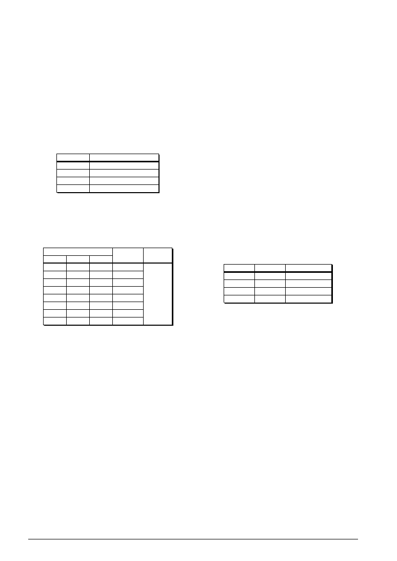
Table 5.15.4.1 Correspondence between A/D input
terminal and PAD register
Terminal
P14 (AD4)
P15 (AD5)
P16 (AD6)
P17 (AD7)
A/D input control register
PAD4
PAD5
PAD6
PAD7
s Setting the input clock
The A/D conversion clock can be selected from
eight types shown in Table 5.15.4.2. The selection is
done using the PSAD register.
Table 5.15.4.2 Input clock selection
Division
ratio
fOSC1/1
fOSC3/64
fOSC3/32
fOSC3/16
fOSC3/8
fOSC3/4
fOSC3/2
fOSC3/1
Output
control
PRAD
register
"1": ON
"0": OFF
PSAD2
1
0
Selection register
PSAD1
1
0
1
0
PSAD0
1
0
1
0
1
0
1
0
The selected clock is input to the A/D converter by
writing "1" to the PRAD register.
Note: When the OSC3 oscillation circuit is made
the clock source, it is necessary to turn the
OSC3 oscillation ON, prior to using the
A/D converter.
From the time the OSC3 oscillation circuit
is turning ON until oscillation stabilizes, an
interval of several msec to several 10
msec is necessary. Consequently, you
should allow an adequate waiting time
after turning the OSC3 oscillation circuit
ON before starting the count of the
programmable timer. (The oscillation start
time will vary somewhat depending on the
oscillator and on external parts. Refer to
the oscillation start time example indicated
in Chapter 10, "ELECTRICAL CHARAC-
TERISTICS".)
At initial reset, OSC3 oscillation circuit is
set to OFF status.
The clock division ratio (see Table
5.15.4.2) must be set so that the A/D
conversion clock frequency is 1 MHz or
less. Furthermore, the A/D conversion
clock frequency should be changed
according to the voltage to be used. Refer
to Chapter 10, "ELECTRICAL CHARAC-
TERISTICS".
The input clock should be set when the
A/D converter stops. Changing in the A/D
converter operation may cause a malfunc-
tion.
To prevent malfunction, do not start A/D
conversion (writing to the CHS register)
when the A/D conversion clock is not
being output from the prescaler, and do
not turn the prescaler output clock off
during A/D conversion.
s Selecting the input signal
The analog signals from the AD4 (P14)–AD7 (P17)
terminals are input to the multiplexer, and the
analog input channel for A/D conversion is
selected by software. This selection can be done
using the CHS register as shown in Table 5.15.4.3.
Table 5.15.4.3 Selection of analog input channel
Input channel
AD7
AD6
AD5
AD4
CHS1
1
0
CHS0
1
0
1
0
s A/D conversion operation
An A/D conversion starts by writing data to the
ADRUN register. For example, when performing
A/D conversion using AD7 as the analog input,
write "1" (1, 1) to the CHS register (CHS1, CHS0)
and then write "1" to the ADRUN register. The A/D
input channel is selected and the A/D conversion
starts. However, it is necessary that the P17 termi-
nal has been set as an analog input terminal.
The built-in sample & hold circuit starts sampling
of the analog input specified from tAD after writing.
When the sampling is completed, the held analog
input voltage is converted into a 10-bit digital value
in successive-approximation architecture.
The conversion result is loaded into the ADDR
(ADDR0–ADDR9) register. ADDR0 is the LSB and
ADDR9 is the MSB.
相關(guān)PDF資料 |
PDF描述 |
|---|---|
| S1D13305F00B | 640 X 256 PIXELS CRT CHAR OR GRPH DSPL CTLR, PQFP60 |
| S1D13305F00A | 640 X 256 PIXELS CRT CHAR OR GRPH DSPL CTLR, PQFP60 |
| S1D13600F00A | CRT OR FLAT PNL GRPH DSPL CTLR, PQFP64 |
| S1D13700F02A100 | 320 X 240 PIXELS CRT OR FLAT PNL GRPH DSPL CTLR, PQFP64 |
| S1D13706F00A | 320 X 240 PIXELS CRT OR FLAT PNL GRPH DSPL CTLR, PQFP100 |
相關(guān)代理商/技術(shù)參數(shù) |
參數(shù)描述 |
|---|---|
| S1C8F360F413100 | 功能描述:16位微控制器 - MCU 8-bit Flash 60KB LCD Dr. 51 x 32 RoHS:否 制造商:Texas Instruments 核心:RISC 處理器系列:MSP430FR572x 數(shù)據(jù)總線寬度:16 bit 最大時鐘頻率:24 MHz 程序存儲器大小:8 KB 數(shù)據(jù) RAM 大小:1 KB 片上 ADC:Yes 工作電源電壓:2 V to 3.6 V 工作溫度范圍:- 40 C to + 85 C 封裝 / 箱體:VQFN-40 安裝風(fēng)格:SMD/SMT |
| S1C8F360F513200 | 功能描述:16位微控制器 - MCU 8-bit Flash 60KB LCD Dr. 51 x 32 RoHS:否 制造商:Texas Instruments 核心:RISC 處理器系列:MSP430FR572x 數(shù)據(jù)總線寬度:16 bit 最大時鐘頻率:24 MHz 程序存儲器大小:8 KB 數(shù)據(jù) RAM 大小:1 KB 片上 ADC:Yes 工作電源電壓:2 V to 3.6 V 工作溫度范圍:- 40 C to + 85 C 封裝 / 箱體:VQFN-40 安裝風(fēng)格:SMD/SMT |
| S1C8F626 | 制造商:EPSON 制造商全稱:EPSON 功能描述:8-bit Single Chip Microcomputer |
| S1C-8-S | 制造商:GRIPCO 功能描述: |
| S1CFB | 制造商:Hubbell Wiring Device-Kellems 功能描述:FLOORBOX, SYSTEM ONE, CAST IRON |
發(fā)布緊急采購,3分鐘左右您將得到回復(fù)。