- 您現(xiàn)在的位置:買賣IC網(wǎng) > PDF目錄98068 > S1C6F567D0A0100 MICROCONTROLLER, UUC141 PDF資料下載
參數(shù)資料
| 型號(hào): | S1C6F567D0A0100 |
| 元件分類: | 微控制器/微處理器 |
| 英文描述: | MICROCONTROLLER, UUC141 |
| 封裝: | DIE-141 |
| 文件頁數(shù): | 74/208頁 |
| 文件大小: | 1561K |
| 代理商: | S1C6F567D0A0100 |
第1頁第2頁第3頁第4頁第5頁第6頁第7頁第8頁第9頁第10頁第11頁第12頁第13頁第14頁第15頁第16頁第17頁第18頁第19頁第20頁第21頁第22頁第23頁第24頁第25頁第26頁第27頁第28頁第29頁第30頁第31頁第32頁第33頁第34頁第35頁第36頁第37頁第38頁第39頁第40頁第41頁第42頁第43頁第44頁第45頁第46頁第47頁第48頁第49頁第50頁第51頁第52頁第53頁第54頁第55頁第56頁第57頁第58頁第59頁第60頁第61頁第62頁第63頁第64頁第65頁第66頁第67頁第68頁第69頁第70頁第71頁第72頁第73頁當(dāng)前第74頁第75頁第76頁第77頁第78頁第79頁第80頁第81頁第82頁第83頁第84頁第85頁第86頁第87頁第88頁第89頁第90頁第91頁第92頁第93頁第94頁第95頁第96頁第97頁第98頁第99頁第100頁第101頁第102頁第103頁第104頁第105頁第106頁第107頁第108頁第109頁第110頁第111頁第112頁第113頁第114頁第115頁第116頁第117頁第118頁第119頁第120頁第121頁第122頁第123頁第124頁第125頁第126頁第127頁第128頁第129頁第130頁第131頁第132頁第133頁第134頁第135頁第136頁第137頁第138頁第139頁第140頁第141頁第142頁第143頁第144頁第145頁第146頁第147頁第148頁第149頁第150頁第151頁第152頁第153頁第154頁第155頁第156頁第157頁第158頁第159頁第160頁第161頁第162頁第163頁第164頁第165頁第166頁第167頁第168頁第169頁第170頁第171頁第172頁第173頁第174頁第175頁第176頁第177頁第178頁第179頁第180頁第181頁第182頁第183頁第184頁第185頁第186頁第187頁第188頁第189頁第190頁第191頁第192頁第193頁第194頁第195頁第196頁第197頁第198頁第199頁第200頁第201頁第202頁第203頁第204頁第205頁第206頁第207頁第208頁
S1C6F567 TECHNICAL MANUAL
EPSON
157
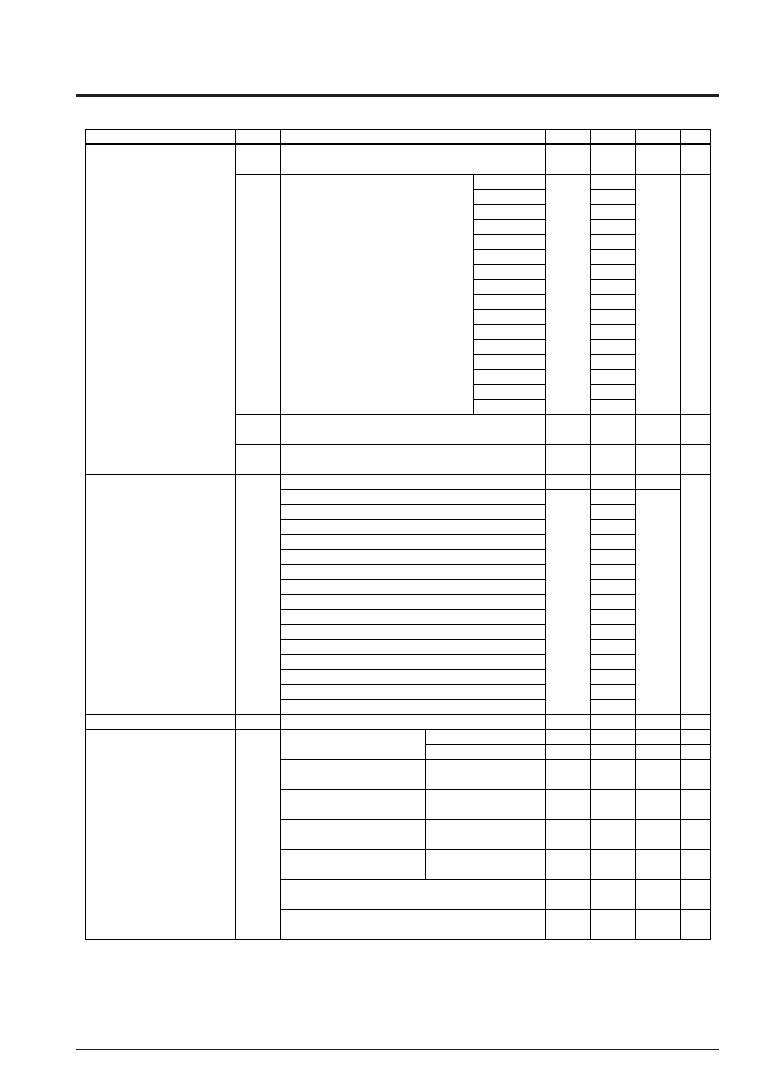
CHAPTER 9: ELECTRICAL CHARACTERISTICS
9.4 Analog Circuit Characteristics and Power Current Consumption
Item
LCD drive voltage
Symbol
VC1
VC23
VC4
VC5
Unit
V
Max.
1/2VC23
×0.95
Typ.
×1.12
3/2VC23
2VC23
Typ.
1.95
1.98
2.01
2.04
2.07
2.10
2.13
2.16
2.19
2.22
2.25
2.28
2.31
2.34
2.37
2.40
Min.
1/2VC23
-0.1
Typ.
×0.88
3/2VC23
×0.95
2VC23
×0.95
Condition
Connect 1 M
load resistor between VSS and VC1
(without panel load)
Connect 1 M
load resistor
LC0–3="0"
between VSS and VC23
LC0–3="1"
(without panel load)
LC0–3="2"
LC0–3="3"
LC0–3="4"
LC0–3="5"
LC0–3="6"
LC0–3="7"
LC0–3="8"
LC0–3="9"
LC0–3="10"
LC0–3="11"
LC0–3="12"
LC0–3="13"
LC0–3="14"
LC0–3="15"
Connect 1 M
load resistor between VSS and VC4
(without panel load)
Connect 1 M
load resistor between VSS and VC5
(without panel load)
Unless otherwise specified:
VDD=3.0V, VSS=0V, fOSC1=32.768kHz, CG=25pF, Ta=25
°C, VD1/VC1/VC23/VC4/VC5 are internal voltage, C1–C8=0.2F
SVD voltage
(Ta=25
°C)
SVD circuit response time
Current consumption
(Ta=25
°C)
1
2
3
VSVD1
tSVD
IOP
V
S
A
mA
A
1.20
Typ.
×1.07
100
150
500
1.5
3.5
65
1.05
–
2.80
2.90
3.00
3.10
3.20
3.30
2.5
12.5
90
300
1
2.3
60
0.95
Typ.
×0.93
Without panel load. The SVD circuit is OFF.
OSCC = "0"
Please input the voltage, which is within the range between VSS and VDD, into the SVD terminal.
SVDS0–3="0" (external)
3
SVDS0–3="1"
SVDS0–3="2"
SVDS0–3="3"
SVDS0–3="4"
SVDS0–3="5"
SVDS0–3="6"
SVDS0–3="7"
SVDS0–3="8"
SVDS0–3="9"
SVDS0–3="10"
SVDS0–3="11"
SVDS0–3="12"
SVDS0–3="13"
SVDS0–3="14"
SVDS0–3="15"
Ta = 25
°C
During HALT
(32 kHz crystal oscillation)
During execution, VDD=3.0V
(32 kHz crystal oscillation)
During execution, VDD=5.0V
(32 kHz crystal oscillation)
During execution, VDD=3.0V
(3.58 MHz ceramic oscillation)
During execution, VDD=5.0V
(3.58 MHz ceramic oscillation)
SVD circuit current (during supply voltage detection)
VDD=3.0V
SVD circuit current (during external voltage detection)
VDD=3.0V
LCD power OFF
1, 2
LCD power ON
1, 2
LCD power ON
相關(guān)PDF資料 |
PDF描述 |
|---|---|
| S1C6N3B0D0A0100 | MICROCONTROLLER, UUC54 |
| S1C6P366D0A0100 | 4-BIT, FLASH, 4.1 MHz, MICROCONTROLLER, UUC102 |
| S1C6P466D0A0A00 | MICROCONTROLLER, UUC140 |
| S1C6S2L7D | 4-BIT, MROM, 0.032 MHz, MICROCONTROLLER, UUC58 |
| S1C6S2A7F | 4-BIT, MROM, 0.08 MHz, MICROCONTROLLER, PQFP60 |
相關(guān)代理商/技術(shù)參數(shù) |
參數(shù)描述 |
|---|---|
| S1C-6-S | 制造商:GRIPCO 功能描述: |
| S1C7309X | 制造商:SAMSUNG 制造商全稱:Samsung semiconductor 功能描述:B/W CCD PROCESSOR |
| S1C7309X01 | 制造商:SAMSUNG 制造商全稱:Samsung semiconductor 功能描述:B/W CCD PROCESSOR |
| S1C88349 | 制造商:EPSON 制造商全稱:EPSON 功能描述:8-bit Single Chip Microcomputer |
| S1C88649 | 制造商:EPSON 制造商全稱:EPSON 功能描述:8-bit Single Chip Microcomputer |
發(fā)布緊急采購(gòu),3分鐘左右您將得到回復(fù)。