- 您現(xiàn)在的位置:買賣IC網(wǎng) > PDF目錄98068 > S1C63406F 4-BIT, MROM, 4.2 MHz, MICROCONTROLLER, PQFP128 PDF資料下載
參數(shù)資料
| 型號(hào): | S1C63406F |
| 元件分類: | 微控制器/微處理器 |
| 英文描述: | 4-BIT, MROM, 4.2 MHz, MICROCONTROLLER, PQFP128 |
| 封裝: | PLASTIC, TQFP15-128 |
| 文件頁(yè)數(shù): | 70/144頁(yè) |
| 文件大小: | 1160K |
| 代理商: | S1C63406F |
第1頁(yè)第2頁(yè)第3頁(yè)第4頁(yè)第5頁(yè)第6頁(yè)第7頁(yè)第8頁(yè)第9頁(yè)第10頁(yè)第11頁(yè)第12頁(yè)第13頁(yè)第14頁(yè)第15頁(yè)第16頁(yè)第17頁(yè)第18頁(yè)第19頁(yè)第20頁(yè)第21頁(yè)第22頁(yè)第23頁(yè)第24頁(yè)第25頁(yè)第26頁(yè)第27頁(yè)第28頁(yè)第29頁(yè)第30頁(yè)第31頁(yè)第32頁(yè)第33頁(yè)第34頁(yè)第35頁(yè)第36頁(yè)第37頁(yè)第38頁(yè)第39頁(yè)第40頁(yè)第41頁(yè)第42頁(yè)第43頁(yè)第44頁(yè)第45頁(yè)第46頁(yè)第47頁(yè)第48頁(yè)第49頁(yè)第50頁(yè)第51頁(yè)第52頁(yè)第53頁(yè)第54頁(yè)第55頁(yè)第56頁(yè)第57頁(yè)第58頁(yè)第59頁(yè)第60頁(yè)第61頁(yè)第62頁(yè)第63頁(yè)第64頁(yè)第65頁(yè)第66頁(yè)第67頁(yè)第68頁(yè)第69頁(yè)當(dāng)前第70頁(yè)第71頁(yè)第72頁(yè)第73頁(yè)第74頁(yè)第75頁(yè)第76頁(yè)第77頁(yè)第78頁(yè)第79頁(yè)第80頁(yè)第81頁(yè)第82頁(yè)第83頁(yè)第84頁(yè)第85頁(yè)第86頁(yè)第87頁(yè)第88頁(yè)第89頁(yè)第90頁(yè)第91頁(yè)第92頁(yè)第93頁(yè)第94頁(yè)第95頁(yè)第96頁(yè)第97頁(yè)第98頁(yè)第99頁(yè)第100頁(yè)第101頁(yè)第102頁(yè)第103頁(yè)第104頁(yè)第105頁(yè)第106頁(yè)第107頁(yè)第108頁(yè)第109頁(yè)第110頁(yè)第111頁(yè)第112頁(yè)第113頁(yè)第114頁(yè)第115頁(yè)第116頁(yè)第117頁(yè)第118頁(yè)第119頁(yè)第120頁(yè)第121頁(yè)第122頁(yè)第123頁(yè)第124頁(yè)第125頁(yè)第126頁(yè)第127頁(yè)第128頁(yè)第129頁(yè)第130頁(yè)第131頁(yè)第132頁(yè)第133頁(yè)第134頁(yè)第135頁(yè)第136頁(yè)第137頁(yè)第138頁(yè)第139頁(yè)第140頁(yè)第141頁(yè)第142頁(yè)第143頁(yè)第144頁(yè)
S1C63406 TECHNICAL MANUAL
EPSON
23
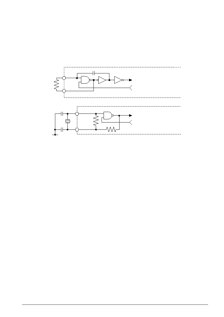
CHAPTER 4: PERIPHERAL CIRCUITS AND OPERATION (Oscillation Circuit)
4.3.3 OSC3 oscillation circuit
The S1C63406 has built-in the OSC3 oscillation circuit that generates the CPU's sub-clock (Max. 4.2 MHz)
for high speed operation and the source clock for peripheral circuits needing a high speed clock (pro-
grammable timer, FOUT output). The mask option enables selection of CR, crystal or ceramic oscillation
circuit.
This circuit operates with the VD1 voltage and the voltage level must be switched when the OSC3 oscilla-
tion is turned ON and OFF (see the next section for details).
Figure 4.3.3.1 is the block diagram of the OSC3 oscillation circuit.
C CR
OSC3
OSC4
R
CR2
VSS
CGC
CDC
Ceramic/
X'tal2
OSC4
OSC3
R
RDC
FC
To CPU
(and some peripheral circuits)
Oscillation circuit control signal
To CPU
(and some peripheral circuits)
Oscillation circuit control signal
(a) CR oscillation circuit
(b) Ceramic/cryctal oscillation circuit
Fig. 4.3.3.1 OSC3 oscillation circuit
As shown in Figure 4.3.3.1, the CR oscillation circuit can be configured simply by connecting the resistor
RCR2 between the OSC3 and OSC4 terminals when CR oscillation is selected. See Chapter 7, "Electrical
Characteristics", for resistance value of RCR2.
When crystal or ceramic oscillation is selected, the crystal or ceramic oscillation circuit can be configured
by connecting a crystal or ceramic oscillator (Max. 4.2 MHz) between the OSC3 and OSC4 terminals,
capacitor CGC between the OSC3 and OSC4 terminals, and capacitor CDC between the OSC4 and VSS
terminals. See Chapter 7, "Electrical Characteristics", for capacitor values of CGC and CDC. To reduce
current consumption of the OSC3 oscillation circuit, oscillation can be stopped by the software (OSCC
register).
相關(guān)PDF資料 |
PDF描述 |
|---|---|
| S1C63408F0A0100 | MICROCONTROLLER, PQFP128 |
| S1C63406D0A0100 | MICROCONTROLLER, UUC103 |
| S1C63455F | 4-BIT, MROM, 4.1 MHz, MICROCONTROLLER, PQFP128 |
| S1C63455D | 4-BIT, MROM, 4.1 MHz, MICROCONTROLLER, UUC105 |
| S1C63458F0A0100 | MICROCONTROLLER, PQFP144 |
相關(guān)代理商/技術(shù)參數(shù) |
參數(shù)描述 |
|---|---|
| S1C63408 | 制造商:EPSON 制造商全稱:EPSON 功能描述:4-bit Single Chip Microcomputer |
| S1C63557D04Q000 | 制造商:Seiko Instruments Inc (SII) 功能描述:EPSON MCU 4BIT |
| S1C63567 | 制造商:EPSON 制造商全稱:EPSON 功能描述:4-bit Single Chip Microcomputer |
| S1C63616 | 制造商:EPSON 制造商全稱:EPSON 功能描述:4-bit Single Chip Microcomputer |
| S1C63632 | 制造商:EPSON 制造商全稱:EPSON 功能描述:4-bit Single Chip Microcomputer |
發(fā)布緊急采購(gòu),3分鐘左右您將得到回復(fù)。