- 您現(xiàn)在的位置:買賣IC網(wǎng) > PDF目錄45010 > M30240M4-XXXFP 16-BIT, MROM, MICROCONTROLLER, PQFP80 PDF資料下載
參數(shù)資料
| 型號: | M30240M4-XXXFP |
| 元件分類: | 微控制器/微處理器 |
| 英文描述: | 16-BIT, MROM, MICROCONTROLLER, PQFP80 |
| 封裝: | 0.80 MM PITCH, PLASTIC, QFP-80 |
| 文件頁數(shù): | 117/125頁 |
| 文件大小: | 753K |
| 代理商: | M30240M4-XXXFP |
第1頁第2頁第3頁第4頁第5頁第6頁第7頁第8頁第9頁第10頁第11頁第12頁第13頁第14頁第15頁第16頁第17頁第18頁第19頁第20頁第21頁第22頁第23頁第24頁第25頁第26頁第27頁第28頁第29頁第30頁第31頁第32頁第33頁第34頁第35頁第36頁第37頁第38頁第39頁第40頁第41頁第42頁第43頁第44頁第45頁第46頁第47頁第48頁第49頁第50頁第51頁第52頁第53頁第54頁第55頁第56頁第57頁第58頁第59頁第60頁第61頁第62頁第63頁第64頁第65頁第66頁第67頁第68頁第69頁第70頁第71頁第72頁第73頁第74頁第75頁第76頁第77頁第78頁第79頁第80頁第81頁第82頁第83頁第84頁第85頁第86頁第87頁第88頁第89頁第90頁第91頁第92頁第93頁第94頁第95頁第96頁第97頁第98頁第99頁第100頁第101頁第102頁第103頁第104頁第105頁第106頁第107頁第108頁第109頁第110頁第111頁第112頁第113頁第114頁第115頁第116頁當(dāng)前第117頁第118頁第119頁第120頁第121頁第122頁第123頁第124頁第125頁
Mitsubishi microcomputers
M16C / 24 Group
SINGLE-CHIP 16-BIT CMOS MICROCOMPUTER
93
CONFIDENTIAL
Preliminary Specifications REV.B
Specifications in this manual are tentative and subject to change
UART0 through UART2
(c) Transfer clock output from multiple pins function (UART1)
This function allows the setting two transfer clock output pins and choosing one of the two to output a clock
by using the CLK and CLKS select bit (bits 4 and 5 at address 03B016). (SeeFigure 86.) The multiple pins
function is valid only when the internal clock is selected for UART1. Note that when this function is selected,
UART1 CTS/RTS function cannot be used.
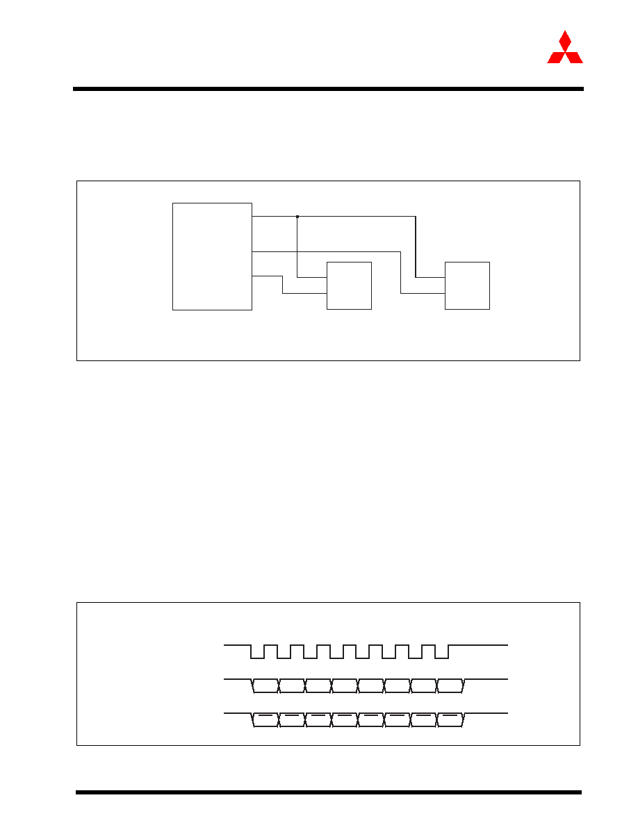
Figure 86:
The transfer clock output from the multiple pins function usage
(d) Continuous receive mode
If the continuous receive mode enable bit (bits 2 and 3 at address 03B016, bit 5 at address 037D16) is set to
“1”, the unit is placed in continuous receive mode. In this mode, when the receive buffer register is read out,
the unit simultaneously goes to a receive enable state without having to set dummy data to the transmit buffer
register back again.
(e) Separate CTS/RTS pins function (UART0)
This function works the same way as in the clock asynchronous serial I/O (UART) mode. The method of set-
ting and the input/output pin functions are both the same, so refer to select function in the next section, “(2)
Clock asynchronous serial I/O (UART) mode.” Note that this function is invalid if the transfer clock output from
the multiple pins function is selected.
(f) Serial data logic switch function (UART2)
When the data logic select bit (bit6 at address 037D16) = “1”, and writing to transmit buffer register or reading
from receive buffer register, data is reversed. Figure 87 shows the example of serial data logic switch timing.
Figure 87:
Serial data logic switch timing
Microcomputer
TXD1 (P67)
CLKS1 (P64)
CLK1 (P65)
IN
CLK
IN
CLK
Note: This applies when the internal clock is selected and transmission
is performed only in clock synchronous serial I/O mode.
D0
D1
D2
D3
D4
D5
D6
D7
D0
D1
D2
D3
D4
D5
D6
D7
Transfer clock
TxD2
(no reverse)
TxD2
(reverse)
“H”
“L”
“H”
“L”
“H”
“L”
When LSB first
相關(guān)PDF資料 |
PDF描述 |
|---|---|
| M30240M1-XXXFP | 16-BIT, MROM, MICROCONTROLLER, PQFP80 |
| M30245MC-XXXGP | 16-BIT, MROM, 16 MHz, MICROCONTROLLER, PQFP100 |
| M30245FCGP | 16-BIT, FLASH, 16 MHz, MICROCONTROLLER, PQFP100 |
| M30260F3VGP | 16-BIT, FLASH, 20 MHz, MICROCONTROLLER, PQFP48 |
| M30260M3A-XXXGP-U5 | 16-BIT, FLASH, 20 MHz, MICROCONTROLLER, PQFP48 |
相關(guān)代理商/技術(shù)參數(shù) |
參數(shù)描述 |
|---|---|
| M30240M5 | 制造商:MITSUBISHI 制造商全稱:Mitsubishi Electric Semiconductor 功能描述:SINGLE-CHIP 16-BIT CMOS MICROCOMPUTER |
| M30240M5-XXXFP | 制造商:MITSUBISHI 制造商全稱:Mitsubishi Electric Semiconductor 功能描述:SINGLE-CHIP 16-BIT CMOS MICROCOMPUTER |
| M30240M6 | 制造商:MITSUBISHI 制造商全稱:Mitsubishi Electric Semiconductor 功能描述:SINGLE-CHIP 16-BIT CMOS MICROCOMPUTER |
| M30240M6-XXXFP | 制造商:MITSUBISHI 制造商全稱:Mitsubishi Electric Semiconductor 功能描述:SINGLE-CHIP 16-BIT CMOS MICROCOMPUTER |
| M30240M7 | 制造商:MITSUBISHI 制造商全稱:Mitsubishi Electric Semiconductor 功能描述:SINGLE-CHIP 16-BIT CMOS MICROCOMPUTER |
發(fā)布緊急采購,3分鐘左右您將得到回復(fù)。