- 您現(xiàn)在的位置:買賣IC網(wǎng) > PDF目錄374047 > ADV7324 (Analog Devices, Inc.) Multiformat 216 MHz Video Encoder with Six NSV 14-Bit DACs PDF資料下載
參數(shù)資料
| 型號(hào): | ADV7324 |
| 廠商: | Analog Devices, Inc. |
| 英文描述: | Multiformat 216 MHz Video Encoder with Six NSV 14-Bit DACs |
| 中文描述: | 多格式視頻編碼器216兆赫六噪聲整形的14位DAC |
| 文件頁數(shù): | 34/92頁 |
| 文件大小: | 992K |
| 代理商: | ADV7324 |
第1頁第2頁第3頁第4頁第5頁第6頁第7頁第8頁第9頁第10頁第11頁第12頁第13頁第14頁第15頁第16頁第17頁第18頁第19頁第20頁第21頁第22頁第23頁第24頁第25頁第26頁第27頁第28頁第29頁第30頁第31頁第32頁第33頁當(dāng)前第34頁第35頁第36頁第37頁第38頁第39頁第40頁第41頁第42頁第43頁第44頁第45頁第46頁第47頁第48頁第49頁第50頁第51頁第52頁第53頁第54頁第55頁第56頁第57頁第58頁第59頁第60頁第61頁第62頁第63頁第64頁第65頁第66頁第67頁第68頁第69頁第70頁第71頁第72頁第73頁第74頁第75頁第76頁第77頁第78頁第79頁第80頁第81頁第82頁第83頁第84頁第85頁第86頁第87頁第88頁第89頁第90頁第91頁第92頁
ADV7324
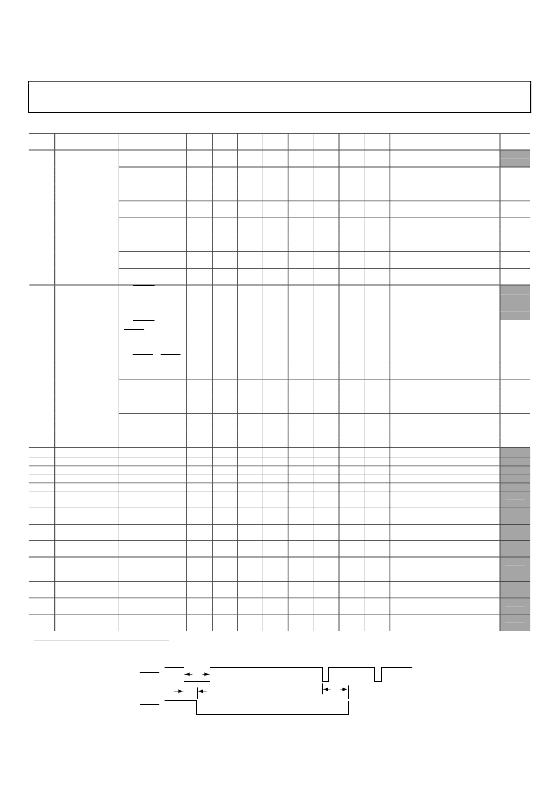
Table 17. Registers 0x4A to 0x58
SR7–
SR0
Register
0x4A
Rev. 0 | Page 34 of 92
Bit Description
SD Slave/Master
Mode
SD Timing Mode
SD BLANK Input
Bit 7
x
Bit 6
0
1
0
Bit 5
0
0
1
1
0
Bit 4
0
1
0
1
0
Bit 3
0
1
0
Bit 2
0
0
1
1
0
Bit 1
0
1
0
1
0
Bit 0
0
1
0
Register Setting
Slave mode.
Master mode.
Mode 0.
Mode 1.
Mode 2.
Mode 3.
Enabled.
Disabled.
No delay.
2 clock cycles.
4 clock cycles.
6 clock cycles.
40 IRE.
7.5 IRE.
A low-high-low transition resets
the internal SD timing counters.
T
a
= 1 clock cycle.
T
a
= 4 clock cycles.
T
a
= 16 clock cycles.
T
a
= 128 clock cycles.
T
b
= 0 clock cycle.
T
b
= 4 clock cycles.
T
b
= 8 clock cycles.
T
b
= 18 clock cycles.
T
c
= T
b
.
T
c
= T
b
+ 32 μs.
Reset
Value
0x08
SD Luma Delay
SD Min. Luma
Value
SD Timing Reset
SD Timing
Register 0
0x4B
SD HSYNC Width
SD HSYNC to
VSYNC Delay
x
x
0
1
0
0
1
1
0
1
0
1
0
0
1
1
0
1
0
1
0x00
SD HSYNC to VSYNC
Rising Edge Delay
(Mode 1 Only)
VSYNC Width
(Mode 2 Only)
0x4C
0x4D
0x4E
0x4F
0x50
0x51
0
0
1
1
x
x
x
x
x
x
0
1
0
1
x
x
x
x
x
x
0
0
1
1
x
x
x
x
x
x
0
1
0
1
x
x
x
x
x
x
x
x
x
x
x
x
x
x
x
x
x
x
x
x
x
x
x
x
x
x
x
x
x
x
1 clock cycle.
4 clock cycles.
16 clock cycles.
128 clock cycles.
0 clock cycles.
1 clock cycle.
2 clock cycles.
3 clock cycles.
Subcarrier Frequency Bit 7 to Bit 0.
Subcarrier Frequency Bit 15 to Bit 8.
Subcarrier Frequency Bit 23 to Bit 16.
Subcarrier Frequency Bit 31 to Bit 24.
Subcarrier Phase Bit 9 to Bit 2.
Extended Data Bit 7 to Bit 0.
0x1E
1
0x7C
0xF0
0x21
0x00
0x00
SD Timing
Register 1
HSYNC to Pixel
Data Adjust
SD F
SC
Register 0
1
SD F
SC
Register 1
SD F
SC
Register 2
SD F
SC
Register 3
SD F
SC
Phase
SD Closed
Captioning
SD Closed
Captioning
SD Closed
Captioning
SD Closed
Captioning
SD Pedestal
Register 0
Extended Data on
Even Fields
Extended Data on
Even Fields
Data on Odd Fields
0x52
x
x
x
x
x
x
x
x
Extended Data Bit 15 to Bit 8.
0x00
0x53
x
x
x
x
x
x
x
x
Data Bit 7 to Bit 0.
0x00
0x54
Data on Odd Fields
x
x
x
x
x
x
x
x
Data Bit 15 to Bit 8.
0x00
0x55
Pedestal on Odd
Fields
17
16
15
14
13
12
11
10
Setting any of these bits to 1
disables pedestal on the line num-
ber indicated by the bit settings.
0x00
0x56
SD Pedestal
Register 1
SD Pedestal
Register 2
SD Pedestal
Register 3
Pedestal on Odd
Fields
Pedestal on Even
Fields
Pedestal on Even
Fields
25
24
23
22
21
20
19
18
0x00
0x57
17
16
15
14
13
12
11
10
0x00
0x58
25
24
23
22
21
20
19
18
0x00
1
For precise NTSC Fsc, this register should be programmed to 0x1F.
LINE 313
LINE 314
LINE 1
T
b
T
a
T
c
0
HSYNC
VSYNC
Figure 47. Timing Register 1 in PAL Mode
相關(guān)PDF資料 |
PDF描述 |
|---|---|
| ADV7324KSTZ | Multiformat 216 MHz Video Encoder with Six NSV 14-Bit DACs |
| ADV7340 | Multiformat Video Encoder, Six 12-Bit Noise Shaped Video㈢ DACS |
| ADV7340BSTZ | Multiformat Video Encoder, Six 12-Bit Noise Shaped Video㈢ DACS |
| ADV7340EBZ | Multiformat Video Encoder, Six 12-Bit Noise Shaped Video㈢ DACS |
| ADV7341 | Multiformat Video Encoder, Six 12-Bit Noise Shaped Video㈢ DACS |
相關(guān)代理商/技術(shù)參數(shù) |
參數(shù)描述 |
|---|---|
| ADV7324KSTZ | 制造商:Analog Devices 功能描述:Video Encoder 64-Pin LQFP |
| ADV7330 | 制造商:AD 制造商全稱:Analog Devices 功能描述:Multiformat 11-Bit Triple DAC Video Encoder |
| ADV73305502 | 制造商:LG Corporation 功能描述:FRAME ASSEMBLY |
| ADV73306701 | 制造商:LG Corporation 功能描述:Frame Assembly |
| ADV73306702 | 制造商:LG Corporation 功能描述:Frame Assembly |
發(fā)布緊急采購,3分鐘左右您將得到回復(fù)。