- 您現(xiàn)在的位置:買賣IC網(wǎng) > PDF目錄374047 > ADV7324 (Analog Devices, Inc.) Multiformat 216 MHz Video Encoder with Six NSV 14-Bit DACs PDF資料下載
參數(shù)資料
| 型號(hào): | ADV7324 |
| 廠商: | Analog Devices, Inc. |
| 英文描述: | Multiformat 216 MHz Video Encoder with Six NSV 14-Bit DACs |
| 中文描述: | 多格式視頻編碼器216兆赫六噪聲整形的14位DAC |
| 文件頁數(shù): | 26/92頁 |
| 文件大?。?/td> | 992K |
| 代理商: | ADV7324 |
第1頁第2頁第3頁第4頁第5頁第6頁第7頁第8頁第9頁第10頁第11頁第12頁第13頁第14頁第15頁第16頁第17頁第18頁第19頁第20頁第21頁第22頁第23頁第24頁第25頁當(dāng)前第26頁第27頁第28頁第29頁第30頁第31頁第32頁第33頁第34頁第35頁第36頁第37頁第38頁第39頁第40頁第41頁第42頁第43頁第44頁第45頁第46頁第47頁第48頁第49頁第50頁第51頁第52頁第53頁第54頁第55頁第56頁第57頁第58頁第59頁第60頁第61頁第62頁第63頁第64頁第65頁第66頁第67頁第68頁第69頁第70頁第71頁第72頁第73頁第74頁第75頁第76頁第77頁第78頁第79頁第80頁第81頁第82頁第83頁第84頁第85頁第86頁第87頁第88頁第89頁第90頁第91頁第92頁
ADV7324
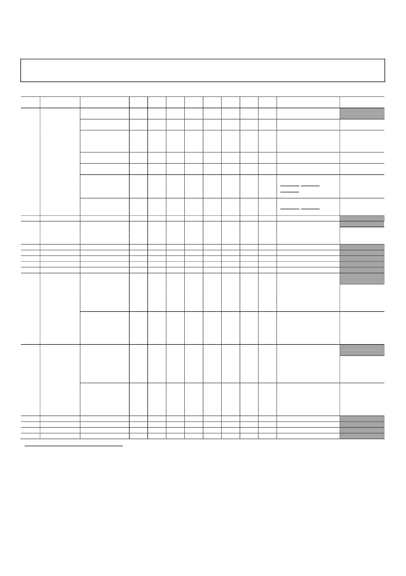
Table 8. Registers 0x02 to 0x0F
SR7–
SR0
Register
0x02
Mode Register 0
Rev. 0 | Page 26 of 92
Bit Description
Reserved
Bit 7
Bit 6
Bit 5
Bit 4
Bit 3
Bit 2
Bit 1
0
Bit 0
0
Register Setting
Zero must be written to
these bits.
Disabled.
Enabled.
Disable manual RGB matrix
adjust.
Enable manual RGB matrix
adjust.
No sync.
Sync on all RGB outputs.
RGB component outputs.
YPrPb component outputs.
No sync output.
Output SD syncs on
S_HSYNC, S_VSYNC,
S_BLANK pins.
No sync output.
Output HD, ED, syncs on
S_HSYNC, S_VSYNC.
LSB for GY.
LSB for RV.
LSB for BU.
LSB for GV.
LSB for GU.
Bit 9 to Bit 2 for GY.
Bit 9 to Bit 2 for GU.
Bit 9 to Bit 2 for GV.
Bit 9 to Bit 2 for BU.
Bit 9 to Bit 2 for RV.
0%
Reset Value
0x20
Test Pattern Black Bar
Manual RGB Matrix
Adjust
0
0
1
0x11, Bit 2 must
also be enabled.
1
Sync on RGB
1
RGB/YPrPb Output
SD Sync
0
1
0
1
0
1
HD Sync
0
1
0x03
0x04
RGB Matrix 0
RGB Matrix 1
x
x
x
x
x
x
0
x
x
x
x
x
x
0
x
x
x
x
x
x
0
x
x
x
x
x
x
0
x
x
x
x
x
x
0
x
x
x
x
x
x
0
x
x
x
x
x
x
x
0
x
x
x
x
x
x
x
0
0x03
0xF0
0x4E
0x0E
0x24
0x92
0x7C
0x00
0x05
0x06
0x07
0x08
0x09
0x0A
RGB Matrix 2
RGB Matrix 3
RGB Matrix 4
RGB Matrix 5
RGB Matrix 6
DAC A, B, C
Output Level
2
Positive Gain to DAC
Output Voltage
Negative Gain to
DAC Output Voltage
Positive Gain to DAC
Output Voltage
Negative Gain to
DAC Output Voltage
Reserved
Reserved
0
0
0
0
1
0
0
0
1
1
0
0
1
0
0
0
0
1
0
0
0
0
1
0
0
0
0
1
0
0
0
1
1
0
0
1
0
…
1
0
0
+0.018%
+0.036%
…
+7.382%
+7.5%
7.5%
0x0B
DAC D, E, F
Output Level
1
1
1
0
1
0
1
0
0
0
1
0
0
0
1
0
0
0
1
0
0
0
1
0
0
1
1
0
1
0
…
1
0
7.382%
7.364%
…
0.018%
0%
0x00
0
0
0
0
1
0
0
0
1
1
0
0
1
0
0
0
0
1
0
0
0
0
1
0
0
0
0
1
0
0
0
1
1
0
0
1
0
…
1
0
0
+0.018%
+0.036%
…
+7.382%
+7.5%
7.5%
0x0C
3
0x0D
3
0x0E
0x0F
1
1
1
0
1
1
0
1
0
1
0
0
1
1
0
0
0
1
1
0
0
0
1
0
0
0
0
1
0
0
0
1
1
1
0
1
0
…
1
1
0
7.382%
7.364%
…
0.018%
0x00
0x00
0x00
0x00
1
For more detail, refer to Appendix 7.
2
For more detail on the programmable output levels, refer to the Programmable DAC Gain Control section.
3
The register setting value must be written after power-up/reset.
相關(guān)PDF資料 |
PDF描述 |
|---|---|
| ADV7324KSTZ | Multiformat 216 MHz Video Encoder with Six NSV 14-Bit DACs |
| ADV7340 | Multiformat Video Encoder, Six 12-Bit Noise Shaped Video㈢ DACS |
| ADV7340BSTZ | Multiformat Video Encoder, Six 12-Bit Noise Shaped Video㈢ DACS |
| ADV7340EBZ | Multiformat Video Encoder, Six 12-Bit Noise Shaped Video㈢ DACS |
| ADV7341 | Multiformat Video Encoder, Six 12-Bit Noise Shaped Video㈢ DACS |
相關(guān)代理商/技術(shù)參數(shù) |
參數(shù)描述 |
|---|---|
| ADV7324KSTZ | 制造商:Analog Devices 功能描述:Video Encoder 64-Pin LQFP |
| ADV7330 | 制造商:AD 制造商全稱:Analog Devices 功能描述:Multiformat 11-Bit Triple DAC Video Encoder |
| ADV73305502 | 制造商:LG Corporation 功能描述:FRAME ASSEMBLY |
| ADV73306701 | 制造商:LG Corporation 功能描述:Frame Assembly |
| ADV73306702 | 制造商:LG Corporation 功能描述:Frame Assembly |
發(fā)布緊急采購,3分鐘左右您將得到回復(fù)。