- 您現(xiàn)在的位置:買賣IC網(wǎng) > PDF目錄375050 > XQ4005E (Xilinx, Inc.) High-Reliability Field Programmable Gate Arrays(高可靠性現(xiàn)場可編程門陣列) PDF資料下載
參數(shù)資料
| 型號: | XQ4005E |
| 廠商: | Xilinx, Inc. |
| 英文描述: | High-Reliability Field Programmable Gate Arrays(高可靠性現(xiàn)場可編程門陣列) |
| 中文描述: | 高可靠性的現(xiàn)場可編程門陣列(高可靠性現(xiàn)場可編程門陣列) |
| 文件頁數(shù): | 26/34頁 |
| 文件大?。?/td> | 529K |
| 代理商: | XQ4005E |
第1頁第2頁第3頁第4頁第5頁第6頁第7頁第8頁第9頁第10頁第11頁第12頁第13頁第14頁第15頁第16頁第17頁第18頁第19頁第20頁第21頁第22頁第23頁第24頁第25頁當前第26頁第27頁第28頁第29頁第30頁第31頁第32頁第33頁第34頁
QPRO
TM
XQ4000E/EX QML High-Reliability Field Programmable Gate Arrays
26
May 19, 1998 (Version 2.1)
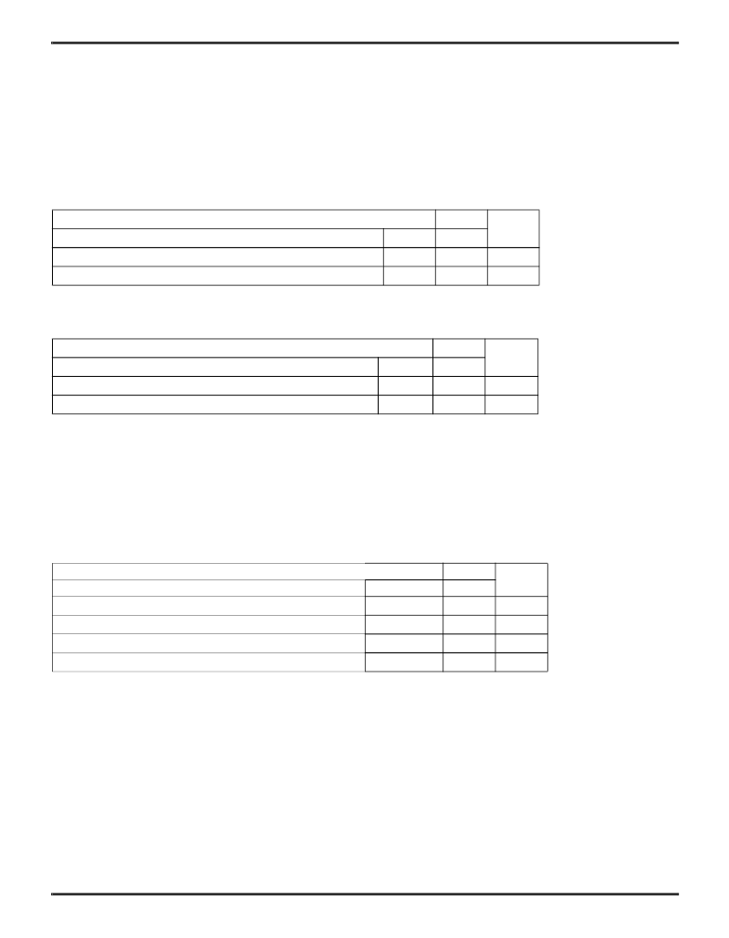
XQ4028EX Pin-to-Pin Output Parameter Guidelines
Testing of switching parameters is modeled after testing methods specified by MIL-M-38510/605. All devices are 100%
functionally tested. Pin-to-pin timing parameters are derived from measuring external and internal test patterns and are
guaranteed over worst-case operating conditions (supply voltage and junction temperature). Listed below are representative
values for typical pin locations and normal clock loading. For more specific, more precise, and worst-case guaranteed data,
reflecting the actual routing structure, use the values provided by the static timing analyzer (TRCE in the Xilinx Development
System) and back-annotated to the simulation netlist. These path delays, provided as a guideline, have been extracted from
the static timing analyzer report. Values apply to all XQ4000EX devices unless otherwise noted.
XQ4028EX Output Flip-Flop, Clock to Out
XQ4028EX Output MUX, Clock to Out
Note 1: Listed above are representative values where one global clock input drives one vertical clock line in each accessible column, and
where all accessible IOB and CLB flip-flops are clocked by the global clock net.
Note 2: Output timing is measured at TTL threshold with 50 pF external capacitive load.
Note 3: Set-up time is measured with the fastest route and the lightest load. Hold time is measured using the farthest distance and a refer-
ence load of one clock pin per two IOBs. Use the static timing analyzer to determine the setup and hold times under given design
conditions.
XQ4028EX Output Level and Slew Rate Adjustments
The following table must be used to adjust output parameters and output switching characteristics.
Speed Grade
Description
Global Low Skew Clock to TTL Output (fast) using OFF
Global Early Clock to TTL Output (fast) using OFF
OFF = Output Flip Flop
-4
Units
Symbol
T
ICKOF
T
ICKEOF
Max
16.6
13.1
ns
ns
Speed Grade
Description
Global Low Skew Clock to TTL Output (fast) using OMUX
Global Early Clock to TTL Output (fast) using OMUX
OMUX = Output MUX
-4
Units
Symbol
T
PFPF
T
PEFPF
Max
15.9
12.4
ns
ns
Speed Grade
Symbol
T
TTLOF
T
TTLO
T
CMOSOF
T
CMOSO
-4
Units
ns
ns
ns
ns
Description
Max
0
2.9
1.0
3.6
For TTL output FAST add
For TTL output SLOW add
For CMOS FAST output add
For CMOS SLOW output add
相關PDF資料 |
PDF描述 |
|---|---|
| XQ4013XL-1CB240N | QML High-Reliability FPGAs |
| XQ4000XL | QML High-Reliability FPGAs |
| XQ4013XL-1BG228M | QML High-Reliability FPGAs |
| XQ4013XL-1BG228N | QML High-Reliability FPGAs |
| XQ4013XL-1BG240M | QML High-Reliability FPGAs |
相關代理商/技術參數(shù) |
參數(shù)描述 |
|---|---|
| XQ4005E-3BG191M | 制造商:XILINX 制造商全稱:XILINX 功能描述:QML High-Reliability FPGAs |
| XQ4005E-3BG191N | 制造商:XILINX 制造商全稱:XILINX 功能描述:QML High-Reliability FPGAs |
| XQ4005E-3BG196M | 制造商:XILINX 制造商全稱:XILINX 功能描述:QML High-Reliability FPGAs |
| XQ4005E-3BG196N | 制造商:XILINX 制造商全稱:XILINX 功能描述:QML High-Reliability FPGAs |
| XQ4005E-3CB191M | 制造商:XILINX 制造商全稱:XILINX 功能描述:QML High-Reliability FPGAs |
發(fā)布緊急采購,3分鐘左右您將得到回復。