- 您現(xiàn)在的位置:買賣IC網(wǎng) > PDF目錄375050 > XQ4005E (Xilinx, Inc.) High-Reliability Field Programmable Gate Arrays(高可靠性現(xiàn)場可編程門陣列) PDF資料下載
參數(shù)資料
| 型號: | XQ4005E |
| 廠商: | Xilinx, Inc. |
| 英文描述: | High-Reliability Field Programmable Gate Arrays(高可靠性現(xiàn)場可編程門陣列) |
| 中文描述: | 高可靠性的現(xiàn)場可編程門陣列(高可靠性現(xiàn)場可編程門陣列) |
| 文件頁數(shù): | 16/34頁 |
| 文件大小: | 529K |
| 代理商: | XQ4005E |
第1頁第2頁第3頁第4頁第5頁第6頁第7頁第8頁第9頁第10頁第11頁第12頁第13頁第14頁第15頁當(dāng)前第16頁第17頁第18頁第19頁第20頁第21頁第22頁第23頁第24頁第25頁第26頁第27頁第28頁第29頁第30頁第31頁第32頁第33頁第34頁
QPRO
TM
XQ4000E/EX QML High-Reliability Field Programmable Gate Arrays
16
May 19, 1998 (Version 2.1)
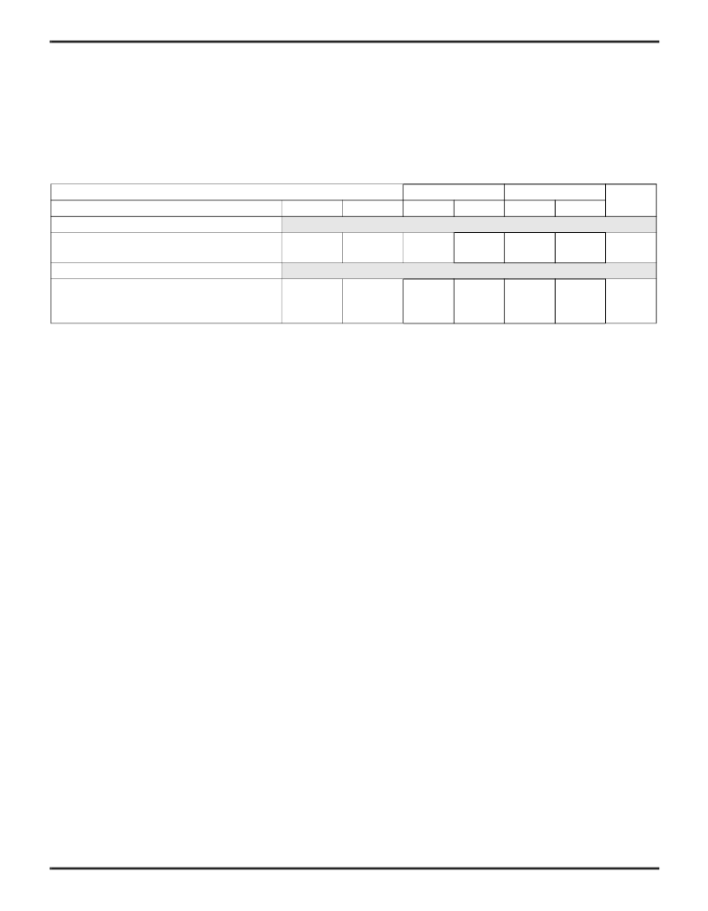
XQ4000E IOB Output Switching Characteristic Guidelines (continued)
Testing of switching parameters is modeled after testing methods specified by MIL-M-38510/605. All devices are 100%
functionally tested. Internal timing parameters are derived from measuring internal test patterns. Listed below are
representative values. For more specific, more precise, and worst-case guaranteed data, use the values reported by the
static timing analyzer (TRCE in the Xilinx Development System) and back-annotated to the simulation netlist. These path
delays, provided as a guideline, have been extracted from the static timing analyzer report. All timing parameters assume
worst-case operating conditions (supply voltage and junction temperature). For Propagation Delays, slew-rate = fast unless
otherwise noted. Values apply to all XQ4000E/EX devices unless otherwise noted.
Note 1:
Output timing is measured at pin threshold, with 50pF external capacitive loads (incl. test fixture). Slew-rate limited output
rise/fall times are approximately two times longer than fast output rise/fall times. For the effect of capacitive loads on ground
bounce, see the “Additional XQ4000 Data” section of the Programmable Logic Data Book.
Voltage levels of unused pads, bonded or unbonded, must be valid logic levels. Each can be configured with the internal
pull-up (default) or pull-down resistor, or configured as a driven output, or can be driven from an external source.
Timing is based on the XQ4005E. For other devices see the static timing analyzer.
Note 2:
Note 3:
Speed Grade
Symbol
-3
-4
Units
Description
Device
Min
Max
Min
Max
Setup and Hold
Output (O) to clock (OK) setup time
Output (O) to clock (OK) hold time
Clock
Clock High
Clock Low
T
OOK
T
OKO
4.6
0
5.0
0
ns
ns
T
CH
T
CL
4.0
4.0
4.5
4.5
ns
ns
相關(guān)PDF資料 |
PDF描述 |
|---|---|
| XQ4013XL-1CB240N | QML High-Reliability FPGAs |
| XQ4000XL | QML High-Reliability FPGAs |
| XQ4013XL-1BG228M | QML High-Reliability FPGAs |
| XQ4013XL-1BG228N | QML High-Reliability FPGAs |
| XQ4013XL-1BG240M | QML High-Reliability FPGAs |
相關(guān)代理商/技術(shù)參數(shù) |
參數(shù)描述 |
|---|---|
| XQ4005E-3BG191M | 制造商:XILINX 制造商全稱:XILINX 功能描述:QML High-Reliability FPGAs |
| XQ4005E-3BG191N | 制造商:XILINX 制造商全稱:XILINX 功能描述:QML High-Reliability FPGAs |
| XQ4005E-3BG196M | 制造商:XILINX 制造商全稱:XILINX 功能描述:QML High-Reliability FPGAs |
| XQ4005E-3BG196N | 制造商:XILINX 制造商全稱:XILINX 功能描述:QML High-Reliability FPGAs |
| XQ4005E-3CB191M | 制造商:XILINX 制造商全稱:XILINX 功能描述:QML High-Reliability FPGAs |
發(fā)布緊急采購,3分鐘左右您將得到回復(fù)。