- 您現(xiàn)在的位置:買賣IC網(wǎng) > PDF目錄4293 > XC3S200A-4VQ100I (Xilinx Inc)IC FPGA SPARTAN 3 100VQFP PDF資料下載
參數(shù)資料
| 型號: | XC3S200A-4VQ100I |
| 廠商: | Xilinx Inc |
| 文件頁數(shù): | 79/132頁 |
| 文件大小: | 0K |
| 描述: | IC FPGA SPARTAN 3 100VQFP |
| 標(biāo)準包裝: | 90 |
| 系列: | Spartan®-3A |
| LAB/CLB數(shù): | 448 |
| 邏輯元件/單元數(shù): | 4032 |
| RAM 位總計: | 294912 |
| 輸入/輸出數(shù): | 68 |
| 門數(shù): | 200000 |
| 電源電壓: | 1.14 V ~ 1.26 V |
| 安裝類型: | 表面貼裝 |
| 工作溫度: | -40°C ~ 100°C |
| 封裝/外殼: | 100-TQFP |
| 供應(yīng)商設(shè)備封裝: | 100-VQFP(14x14) |
第1頁第2頁第3頁第4頁第5頁第6頁第7頁第8頁第9頁第10頁第11頁第12頁第13頁第14頁第15頁第16頁第17頁第18頁第19頁第20頁第21頁第22頁第23頁第24頁第25頁第26頁第27頁第28頁第29頁第30頁第31頁第32頁第33頁第34頁第35頁第36頁第37頁第38頁第39頁第40頁第41頁第42頁第43頁第44頁第45頁第46頁第47頁第48頁第49頁第50頁第51頁第52頁第53頁第54頁第55頁第56頁第57頁第58頁第59頁第60頁第61頁第62頁第63頁第64頁第65頁第66頁第67頁第68頁第69頁第70頁第71頁第72頁第73頁第74頁第75頁第76頁第77頁第78頁當(dāng)前第79頁第80頁第81頁第82頁第83頁第84頁第85頁第86頁第87頁第88頁第89頁第90頁第91頁第92頁第93頁第94頁第95頁第96頁第97頁第98頁第99頁第100頁第101頁第102頁第103頁第104頁第105頁第106頁第107頁第108頁第109頁第110頁第111頁第112頁第113頁第114頁第115頁第116頁第117頁第118頁第119頁第120頁第121頁第122頁第123頁第124頁第125頁第126頁第127頁第128頁第129頁第130頁第131頁第132頁
DC and Switching Characteristics
50
DS529-3 (v2.0) August 19, 2010
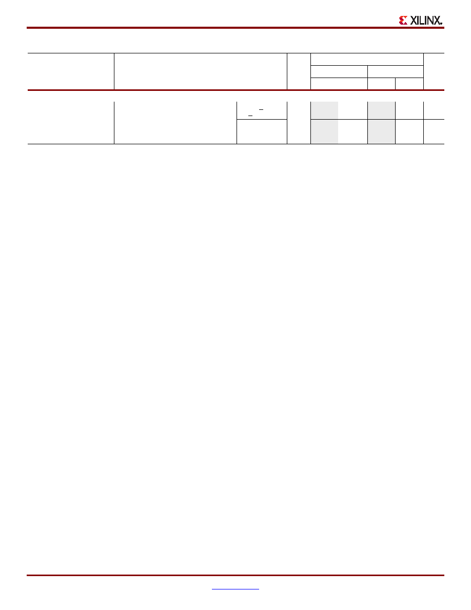
Lock Time
LOCK_FX(2, 3)
The time from deassertion at the DCM’s
Reset input to the rising transition at its
LOCKED output. The DFS asserts
LOCKED when the CLKFX and CLKFX180
signals are valid. If using both the DLL and
the DFS, use the longer locking time.
5 MHz < FCLKIN
< 15 MHz
All
–
5
–
5ms
FCLKIN >
15 MHz
–
450
–
450
s
Notes:
1.
2.
DFS performance requires the additional logic automatically added by ISE 9.1i and later software revisions.
3.
For optimal jitter tolerance and faster lock time, use the CLKIN_PERIOD attribute.
4.
Maximum output jitter is characterized within a reasonable noise environment (150 ps input period jitter, 40 SSOs and 25% CLB switching)
on an XC3S1400A FPGA. Output jitter strongly depends on the environment, including the number of SSOs, the output drive strength, CLB
utilization, CLB switching activities, switching frequency, power supply and PCB design. The actual maximum output jitter depends on the
system application.
5.
The CLKFX and CLKFX180 outputs always have an approximate 50% duty cycle.
6.
Some duty-cycle and alignment specifications include a percentage of the CLKFX output period. For example, the data sheet specifies a
maximum CLKFX jitter of “±[1% of CLKFX period + 200]”. Assume the CLKFX output frequency is 100 MHz. The equivalent CLKFX period
is 10 ns and 1% of 10 ns is 0.1 ns or 100 ps. According to the data sheet, the maximum jitter is ±[100 ps + 200 ps] = ±300 ps.
Table 39: Switching Characteristics for the DFS(Continued)
Symbol
Description
Device
Speed Grade
Units
-5
-4
Min
Max
Min
Max
相關(guān)PDF資料 |
PDF描述 |
|---|---|
| XC3S100E-4TQ144I | IC FPGA SPARTAN 3E 144TQFP |
| XC3S100E-5TQG144C | IC FPGA SPARTAN-3E 100K 144-TQFP |
| XC3S100E-5CPG132C | IC FPGA SPARTAN-3E 100K 132CSBGA |
| XC3S100E-4CPG132I | IC FPGA SPARTAN-3E 100K 132CSBGA |
| 24LC16B-E/ST | IC EEPROM 16KBIT 400KHZ 8TSSOP |
相關(guān)代理商/技術(shù)參數(shù) |
參數(shù)描述 |
|---|---|
| XC3S200A-4VQG100C | 功能描述:IC FPGA SPARTAN-3A 200K 100-VQFP RoHS:是 類別:集成電路 (IC) >> 嵌入式 - FPGA(現(xiàn)場可編程門陣列) 系列:Spartan®-3A 標(biāo)準包裝:40 系列:Spartan® 6 LX LAB/CLB數(shù):3411 邏輯元件/單元數(shù):43661 RAM 位總計:2138112 輸入/輸出數(shù):358 門數(shù):- 電源電壓:1.14 V ~ 1.26 V 安裝類型:表面貼裝 工作溫度:-40°C ~ 100°C 封裝/外殼:676-BGA 供應(yīng)商設(shè)備封裝:676-FBGA(27x27) |
| XC3S200A-4VQG100I | 功能描述:IC FPGA SPARTAN-3A 200K 100-VQFP RoHS:是 類別:集成電路 (IC) >> 嵌入式 - FPGA(現(xiàn)場可編程門陣列) 系列:Spartan®-3A 標(biāo)準包裝:24 系列:ECP2 LAB/CLB數(shù):1500 邏輯元件/單元數(shù):12000 RAM 位總計:226304 輸入/輸出數(shù):131 門數(shù):- 電源電壓:1.14 V ~ 1.26 V 安裝類型:表面貼裝 工作溫度:0°C ~ 85°C 封裝/外殼:208-BFQFP 供應(yīng)商設(shè)備封裝:208-PQFP(28x28) |
| XC3S200A-5FG320C | 功能描述:IC SPARTAN-3A FPGA 200K 320FBGA RoHS:否 類別:集成電路 (IC) >> 嵌入式 - FPGA(現(xiàn)場可編程門陣列) 系列:Spartan®-3A 標(biāo)準包裝:40 系列:Spartan® 6 LX LAB/CLB數(shù):3411 邏輯元件/單元數(shù):43661 RAM 位總計:2138112 輸入/輸出數(shù):358 門數(shù):- 電源電壓:1.14 V ~ 1.26 V 安裝類型:表面貼裝 工作溫度:-40°C ~ 100°C 封裝/外殼:676-BGA 供應(yīng)商設(shè)備封裝:676-FBGA(27x27) |
| XC3S200A-5FGG320C | 功能描述:IC SPARTAN-3A FPGA 200K 320-FBGA RoHS:是 類別:集成電路 (IC) >> 嵌入式 - FPGA(現(xiàn)場可編程門陣列) 系列:Spartan®-3A 標(biāo)準包裝:40 系列:Spartan® 6 LX LAB/CLB數(shù):3411 邏輯元件/單元數(shù):43661 RAM 位總計:2138112 輸入/輸出數(shù):358 門數(shù):- 電源電壓:1.14 V ~ 1.26 V 安裝類型:表面貼裝 工作溫度:-40°C ~ 100°C 封裝/外殼:676-BGA 供應(yīng)商設(shè)備封裝:676-FBGA(27x27) |
| XC3S200A-5FT256C | 功能描述:IC SPARTAN-3A FPGA 200K 256FTBGA RoHS:否 類別:集成電路 (IC) >> 嵌入式 - FPGA(現(xiàn)場可編程門陣列) 系列:Spartan®-3A 標(biāo)準包裝:40 系列:Spartan® 6 LX LAB/CLB數(shù):3411 邏輯元件/單元數(shù):43661 RAM 位總計:2138112 輸入/輸出數(shù):358 門數(shù):- 電源電壓:1.14 V ~ 1.26 V 安裝類型:表面貼裝 工作溫度:-40°C ~ 100°C 封裝/外殼:676-BGA 供應(yīng)商設(shè)備封裝:676-FBGA(27x27) |
發(fā)布緊急采購,3分鐘左右您將得到回復(fù)。