- 您現(xiàn)在的位置:買賣IC網(wǎng) > PDF目錄384797 > OR4E4 (Lineage Power) Field-Programmable Gate Arrays(現(xiàn)場可編程門陣列) PDF資料下載
參數(shù)資料
| 型號: | OR4E4 |
| 廠商: | Lineage Power |
| 英文描述: | Field-Programmable Gate Arrays(現(xiàn)場可編程門陣列) |
| 中文描述: | 現(xiàn)場可編程門陣列(現(xiàn)場可編程門陣列) |
| 文件頁數(shù): | 65/132頁 |
| 文件大?。?/td> | 2667K |
| 代理商: | OR4E4 |
第1頁第2頁第3頁第4頁第5頁第6頁第7頁第8頁第9頁第10頁第11頁第12頁第13頁第14頁第15頁第16頁第17頁第18頁第19頁第20頁第21頁第22頁第23頁第24頁第25頁第26頁第27頁第28頁第29頁第30頁第31頁第32頁第33頁第34頁第35頁第36頁第37頁第38頁第39頁第40頁第41頁第42頁第43頁第44頁第45頁第46頁第47頁第48頁第49頁第50頁第51頁第52頁第53頁第54頁第55頁第56頁第57頁第58頁第59頁第60頁第61頁第62頁第63頁第64頁當前第65頁第66頁第67頁第68頁第69頁第70頁第71頁第72頁第73頁第74頁第75頁第76頁第77頁第78頁第79頁第80頁第81頁第82頁第83頁第84頁第85頁第86頁第87頁第88頁第89頁第90頁第91頁第92頁第93頁第94頁第95頁第96頁第97頁第98頁第99頁第100頁第101頁第102頁第103頁第104頁第105頁第106頁第107頁第108頁第109頁第110頁第111頁第112頁第113頁第114頁第115頁第116頁第117頁第118頁第119頁第120頁第121頁第122頁第123頁第124頁第125頁第126頁第127頁第128頁第129頁第130頁第131頁第132頁
Lucent Technologies Inc.
65
Preliminary Data Sheet
August 2000
ORCA Series 4 FPGAs
FPGA Configuration Modes
(continued)
5-4456(F)
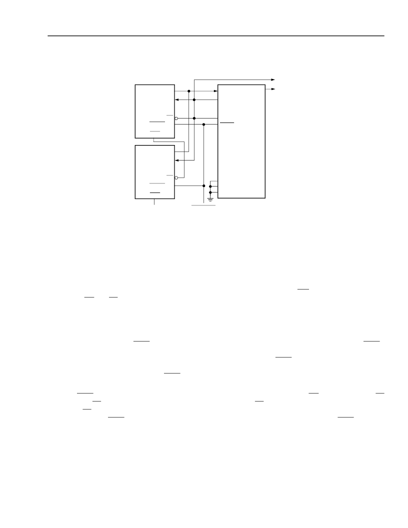
Figure 39. Master Serial Configuration Schematic
Asynchronous Peripheral Mode
Figure 40 shows the connections needed for the asynchronous peripheral mode. In this mode, the FPGA system
interface is similar to that of a microprocessor-peripheral interface. The microprocessor generates the control sig-
nals to write an 8-bit byte into the FPGA. The FPGA control inputs include active-low
CS0
and active-high CS1 chip
selects and
WR
and
RD
inputs. The chip selects can be cycled or maintained at a static level during the configura-
tion cycle. Each byte of data is written into the FPGA’s D[7:0] input pins. D[7:0] of the FPGA can be connected to
D[7:0] of the microprocessor only if a standard prom file format is used. If a .bit or .rbt file is used from ORCA
Foundry, then the user must mirror the bytes in the .bit or .rbt file
or
leave the .bit or .rbt file unchanged and connect
D[7:0] of the FPGA to D[0:7] of the microprocessor.
The FPGA provides an RDY/
BUSY
status output to indicate that another byte can be loaded. A low on RDY/
BUSY
indicates that the double-buffered hold/shift registers are not ready to receive data, and this pin must be monitored
to go high before another byte of data can be written. The shortest time RDY/
BUSY
is low occurs when a byte is
loaded into the hold register and the shift register is empty, in which case the byte is immediately transferred to the
shift register. The longest time for RDY/
BUSY
to remain low occurs when a byte is loaded into the holding register
and the shift register has just started shifting configuration data into configuration RAM.
The RDY/
BUSY
status is also available on the D7 pin by enabling the chip selects, setting
WR
high, and applying
RD
low, where the
RD
input provides an output enable for the D7 pin when
RD
is low. The D[6:0] pins are not enabled to
drive when
RD
is low and, therefore, only act as input pins in asynchronous peripheral mode. Optionally, the user
can ignore the RDY/
BUSY
status and simply wait until the maximum time it would take for the RDY/
BUSY
line to go
high, indicating the FPGA is ready for more data, before writing the next data byte.
DIN
M2
M1
M0
ORCA
SERIES
FPGA
CCLK
DOUT
TO DAISY-
CHAINED
DEVICES
DATA
CLK
CE
CEO
DATA
CLK
RESET/OE
CEO
CE
TO MORE
SERIAL ROMs
AS NEEDED
DONE
PRGM
PROGRAM
RESET/OE
相關PDF資料 |
PDF描述 |
|---|---|
| OR4E6 | Field-Programmable Gate Arrays(現(xiàn)場可編程門陣列) |
| ORT4622 | Field-Programmable System Chip (FPSC) Four Channel x 622 Mbits/s Backplane Transceiver(現(xiàn)場可編程系統(tǒng)芯片(四通道x 622 M位/秒背板收發(fā)器)) |
| ORT8850 | Field-Programmable System Chip(現(xiàn)場可編程系統(tǒng)芯片) |
| OS8740230 | Si Optical Receiver, 40 - 870MHz, 225mA max. @ 24VDC |
| OSC-1A0 | Ultra Miniature TCXO |
相關代理商/技術參數(shù) |
參數(shù)描述 |
|---|---|
| OR4E4-1BA352 | 制造商:未知廠家 制造商全稱:未知廠家 功能描述:FPGA |
| OR4E4-1BA416 | 制造商:未知廠家 制造商全稱:未知廠家 功能描述:FPGA |
| OR4E4-1BC432 | 制造商:未知廠家 制造商全稱:未知廠家 功能描述:FPGA |
| OR4E4-1BM680 | 制造商:未知廠家 制造商全稱:未知廠家 功能描述:FPGA |
| OR4E4-2BA352 | 制造商:未知廠家 制造商全稱:未知廠家 功能描述:FPGA |
發(fā)布緊急采購,3分鐘左右您將得到回復。