- 您現(xiàn)在的位置:買賣IC網(wǎng) > PDF目錄384797 > OR4E4 (Lineage Power) Field-Programmable Gate Arrays(現(xiàn)場(chǎng)可編程門陣列) PDF資料下載
參數(shù)資料
| 型號(hào): | OR4E4 |
| 廠商: | Lineage Power |
| 英文描述: | Field-Programmable Gate Arrays(現(xiàn)場(chǎng)可編程門陣列) |
| 中文描述: | 現(xiàn)場(chǎng)可編程門陣列(現(xiàn)場(chǎng)可編程門陣列) |
| 文件頁數(shù): | 44/132頁 |
| 文件大小: | 2667K |
| 代理商: | OR4E4 |
第1頁第2頁第3頁第4頁第5頁第6頁第7頁第8頁第9頁第10頁第11頁第12頁第13頁第14頁第15頁第16頁第17頁第18頁第19頁第20頁第21頁第22頁第23頁第24頁第25頁第26頁第27頁第28頁第29頁第30頁第31頁第32頁第33頁第34頁第35頁第36頁第37頁第38頁第39頁第40頁第41頁第42頁第43頁當(dāng)前第44頁第45頁第46頁第47頁第48頁第49頁第50頁第51頁第52頁第53頁第54頁第55頁第56頁第57頁第58頁第59頁第60頁第61頁第62頁第63頁第64頁第65頁第66頁第67頁第68頁第69頁第70頁第71頁第72頁第73頁第74頁第75頁第76頁第77頁第78頁第79頁第80頁第81頁第82頁第83頁第84頁第85頁第86頁第87頁第88頁第89頁第90頁第91頁第92頁第93頁第94頁第95頁第96頁第97頁第98頁第99頁第100頁第101頁第102頁第103頁第104頁第105頁第106頁第107頁第108頁第109頁第110頁第111頁第112頁第113頁第114頁第115頁第116頁第117頁第118頁第119頁第120頁第121頁第122頁第123頁第124頁第125頁第126頁第127頁第128頁第129頁第130頁第131頁第132頁
44
Lucent Technologies Inc.
Preliminary Data Sheet
August 2000
ORCA Series 4 FPGAs
Special Function Blocks
(continued)
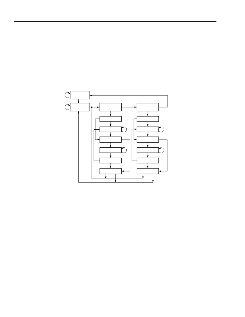
The TAPC generates control signals that allow capture, shift, and update operations on the instruction and data
registers. In the capture operation, data is loaded into the register. In the shift operation, the captured data is
shifted out while new data is shifted in. In the update operation, either the instruction register is loaded for instruc-
tion decode, or the boundary-scan register is updated for control of outputs.
The test host generates a test by providing input into the ORCA Series TMS input synchronous with TCK. This
sequences the TAPC through states in order to perform the desired function on the instruction register or a data
register. Figure 28 provides a diagram of the state transitions for the TAPC. The next state is determined by the
TMS input value.
5-5370(F)
Figure 28. TAP Controller State Transition Diagram
SELECT-
DR-SCAN
CAPTURE-DR
SHIFT-DR
EXIT1-DR
PAUSE-DR
EXIT2-DR
UPDATE-DR
1
1
1
0
0
0
RUN-TEST/
IDLE
1
TEST-LOGIC-
RESET
SELECT-
IR-SCAN
CAPTURE-IR
SHIFT-IR
EXIT1-IR
PAUSE-IR
EXIT2-IR
UPDATE-IR
1
1
1
0
0
0
0
0
0
1
0
1
1
1
0
1
1
0
0
0
0
1
1
1
0
Boundary-Scan Cells
Figure 29 is a diagram of the boundary-scan cell (BSC)
in the ORCA series PIOs. There are four BSCs in each
PIO: one for each pad, except as noted above. The
BSCs are connected serially to form the BSR. The
BSC controls the functionality of the in, out, and 3-state
signals for each pad.
The BSC allows the I/O to function in either the normal
or test mode. Normal mode is defined as when an out-
put buffer receives input from the PLC array and pro-
vides output at the pad or when an input buffer
provides input from the pad to the PLC array. In the test
mode, the BSC executes a boundary-scan operation,
such as shifting in scan data from an upstream BSC in
the BSR, providing test stimuli to the pad, capturing
test data at the pad, etc.
The primary functions of the BSC are shifting scan data
serially in the BSR and observing input (p_in), output
(p_out), and 3-state (p_ts) signals at the pads. The
BSC consists of two circuits: the bidirectional data cell
is used to access the input and output data, and the
direction control cell is used to access the 3-state
value. Both cells consist of a FF used to shift scan data
which feeds a FF to control the I/O buffer. The bidirec-
tional data cell is connected serially to the direction
control cell to form a boundary-scan shift register.
The TAPC signals (capture, update, shiftn, treset, and
TCK) and the MODE signal control the operation of the
BSC. The bidirectional data cell is also controlled by
the high out/low in (HOLI) signal generated by the
direction control cell. When HOLI is low, the bidirec-
tional data cell receives input buffer data into the BSC.
When HOLI is high, the BSC is loaded with functional
data from the PLC.
相關(guān)PDF資料 |
PDF描述 |
|---|---|
| OR4E6 | Field-Programmable Gate Arrays(現(xiàn)場(chǎng)可編程門陣列) |
| ORT4622 | Field-Programmable System Chip (FPSC) Four Channel x 622 Mbits/s Backplane Transceiver(現(xiàn)場(chǎng)可編程系統(tǒng)芯片(四通道x 622 M位/秒背板收發(fā)器)) |
| ORT8850 | Field-Programmable System Chip(現(xiàn)場(chǎng)可編程系統(tǒng)芯片) |
| OS8740230 | Si Optical Receiver, 40 - 870MHz, 225mA max. @ 24VDC |
| OSC-1A0 | Ultra Miniature TCXO |
相關(guān)代理商/技術(shù)參數(shù) |
參數(shù)描述 |
|---|---|
| OR4E4-1BA352 | 制造商:未知廠家 制造商全稱:未知廠家 功能描述:FPGA |
| OR4E4-1BA416 | 制造商:未知廠家 制造商全稱:未知廠家 功能描述:FPGA |
| OR4E4-1BC432 | 制造商:未知廠家 制造商全稱:未知廠家 功能描述:FPGA |
| OR4E4-1BM680 | 制造商:未知廠家 制造商全稱:未知廠家 功能描述:FPGA |
| OR4E4-2BA352 | 制造商:未知廠家 制造商全稱:未知廠家 功能描述:FPGA |
發(fā)布緊急采購,3分鐘左右您將得到回復(fù)。