- 您現(xiàn)在的位置:買賣IC網(wǎng) > PDF目錄45188 > MB90P663AP-SH 16-BIT, OTPROM, 16 MHz, MICROCONTROLLER, PDIP64 PDF資料下載
參數(shù)資料
| 型號: | MB90P663AP-SH |
| 元件分類: | 微控制器/微處理器 |
| 英文描述: | 16-BIT, OTPROM, 16 MHz, MICROCONTROLLER, PDIP64 |
| 封裝: | PLASTIC, SHRINK, DIP-64 |
| 文件頁數(shù): | 157/284頁 |
| 文件大小: | 2703K |
| 代理商: | MB90P663AP-SH |
第1頁第2頁第3頁第4頁第5頁第6頁第7頁第8頁第9頁第10頁第11頁第12頁第13頁第14頁第15頁第16頁第17頁第18頁第19頁第20頁第21頁第22頁第23頁第24頁第25頁第26頁第27頁第28頁第29頁第30頁第31頁第32頁第33頁第34頁第35頁第36頁第37頁第38頁第39頁第40頁第41頁第42頁第43頁第44頁第45頁第46頁第47頁第48頁第49頁第50頁第51頁第52頁第53頁第54頁第55頁第56頁第57頁第58頁第59頁第60頁第61頁第62頁第63頁第64頁第65頁第66頁第67頁第68頁第69頁第70頁第71頁第72頁第73頁第74頁第75頁第76頁第77頁第78頁第79頁第80頁第81頁第82頁第83頁第84頁第85頁第86頁第87頁第88頁第89頁第90頁第91頁第92頁第93頁第94頁第95頁第96頁第97頁第98頁第99頁第100頁第101頁第102頁第103頁第104頁第105頁第106頁第107頁第108頁第109頁第110頁第111頁第112頁第113頁第114頁第115頁第116頁第117頁第118頁第119頁第120頁第121頁第122頁第123頁第124頁第125頁第126頁第127頁第128頁第129頁第130頁第131頁第132頁第133頁第134頁第135頁第136頁第137頁第138頁第139頁第140頁第141頁第142頁第143頁第144頁第145頁第146頁第147頁第148頁第149頁第150頁第151頁第152頁第153頁第154頁第155頁第156頁當(dāng)前第157頁第158頁第159頁第160頁第161頁第162頁第163頁第164頁第165頁第166頁第167頁第168頁第169頁第170頁第171頁第172頁第173頁第174頁第175頁第176頁第177頁第178頁第179頁第180頁第181頁第182頁第183頁第184頁第185頁第186頁第187頁第188頁第189頁第190頁第191頁第192頁第193頁第194頁第195頁第196頁第197頁第198頁第199頁第200頁第201頁第202頁第203頁第204頁第205頁第206頁第207頁第208頁第209頁第210頁第211頁第212頁第213頁第214頁第215頁第216頁第217頁第218頁第219頁第220頁第221頁第222頁第223頁第224頁第225頁第226頁第227頁第228頁第229頁第230頁第231頁第232頁第233頁第234頁第235頁第236頁第237頁第238頁第239頁第240頁第241頁第242頁第243頁第244頁第245頁第246頁第247頁第248頁第249頁第250頁第251頁第252頁第253頁第254頁第255頁第256頁第257頁第258頁第259頁第260頁第261頁第262頁第263頁第264頁第265頁第266頁第267頁第268頁第269頁第270頁第271頁第272頁第273頁第274頁第275頁第276頁第277頁第278頁第279頁第280頁第281頁第282頁第283頁第284頁
2.1 CPU
19
s Type of Bank Addressing
In bank addressing the 16-Mbyte memory space is divided into 256 banks of 64 Kbytes each, with bank
addresses maintained in a system of bank registers. There are five types of bank registers available.
Table 2.1.1 lists bank registers, the space accessed by each register, and principal uses.
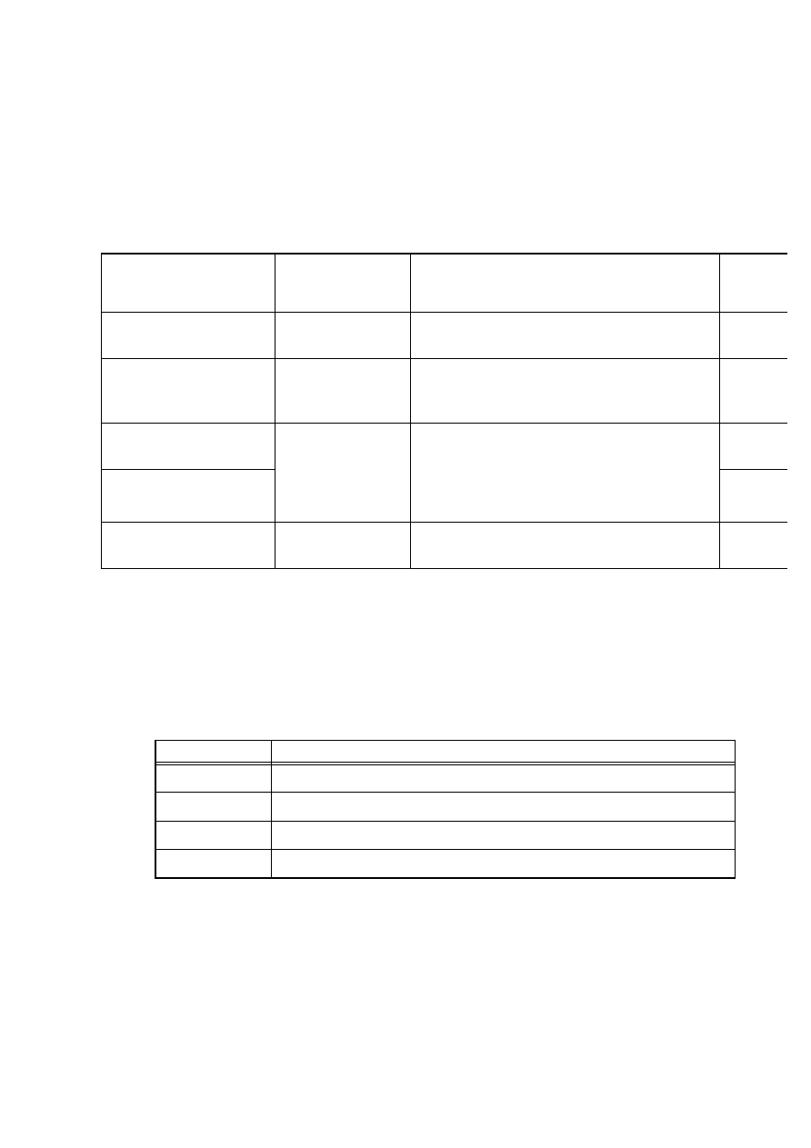
Table 2.1.1 Spaces Accessed by Bank Registers
To enhance coding efficiency, each instruction has defined default spaces for each type of addressing as
shown in Table 2.1.2. When an addressing operation uses a space other than its default space, a prefix
code corresponding to the desired bank is attached to the beginning of the instruction to allow access to
the bank space designated by that prefix code.
Table 2.1.2 Default Spaces
Bank register
Space name
Principal uses
Initial
value at
reset
Program bank register
(PCB)
Program (PC) space
Storage of instruction codes, vector tables, and
immediate data
FFH
Data bank register (DTB)
Data (DT) space
Storage of readable/writable data
Access to internal or external peripheral resource
control registers and data registers
00H
User stack bank register
(USB)
Stack (SP) space
Area used for stack access to registers for saving
of PUSH/POP instructions and interrupt instruc-
tions, etc.
SSB is used when CCR S=1, USB used when
S=0.
00H
System stack bank register
(SSB)
00H
Additional bank register
(ADB)
Additional (AD)
space
Storage of data overflow from data (DT) space
00H
18/ After reset, DT, SP and AD spaces are located in bank 00 (000000H to 00FFFFH), and PC space is
located in bank FF (FF0000H to FFFFFFH).
Default space
Addressing method
Program space
PC indirect, program access, branching
Data space
Addressing using @RW0, @RW1, @RW4, @RW5; @A, addr16, dir
Stack space
Addressing using PUSHW, POPW, @RW3, @RW7
Additional space
Addressing using @RW2, @RW6
相關(guān)PDF資料 |
PDF描述 |
|---|---|
| MB90673PF | 16-BIT, MROM, 16 MHz, MICROCONTROLLER, PQFP80 |
| MB90T673PF | 16-BIT, 16 MHz, MICROCONTROLLER, PQFP80 |
| MB90671PFV | 16-BIT, MROM, 16 MHz, MICROCONTROLLER, PQFP80 |
| MB90671PF | 16-BIT, MROM, 16 MHz, MICROCONTROLLER, PQFP80 |
| MB90P678PF | 16-BIT, OTPROM, 16 MHz, MICROCONTROLLER, PQFP100 |
相關(guān)代理商/技術(shù)參數(shù) |
參數(shù)描述 |
|---|---|
| MB90V340A-102CR | 制造商:FUJITSU 功能描述: |
| MB-910 | 制造商:Circuit Test 功能描述:BREADBOARD WIRING KIT - 350 PCS |
| MB9100100 | 制造商:COM/DUO 功能描述:FAN 4-6WKS |
| MB9100-100 | 制造商:COM/DUO 功能描述:FAN 4-6WKS |
| MB91101 | 制造商:Panasonic Industrial Company 功能描述:IC |
發(fā)布緊急采購,3分鐘左右您將得到回復(fù)。