- 您現(xiàn)在的位置:買(mǎi)賣(mài)IC網(wǎng) > PDF目錄373103 > KBE00F005A (SAMSUNG SEMICONDUCTOR CO. LTD.) 512Mb NAND*2 + 256Mb Mobile SDRAM*2 PDF資料下載
參數(shù)資料
| 型號(hào): | KBE00F005A |
| 廠商: | SAMSUNG SEMICONDUCTOR CO. LTD. |
| 英文描述: | 512Mb NAND*2 + 256Mb Mobile SDRAM*2 |
| 中文描述: | 的512Mb的NAND * 2 256Mb的移動(dòng)SDRAM * 2 |
| 文件頁(yè)數(shù): | 39/87頁(yè) |
| 文件大小: | 1353K |
| 代理商: | KBE00F005A |
第1頁(yè)第2頁(yè)第3頁(yè)第4頁(yè)第5頁(yè)第6頁(yè)第7頁(yè)第8頁(yè)第9頁(yè)第10頁(yè)第11頁(yè)第12頁(yè)第13頁(yè)第14頁(yè)第15頁(yè)第16頁(yè)第17頁(yè)第18頁(yè)第19頁(yè)第20頁(yè)第21頁(yè)第22頁(yè)第23頁(yè)第24頁(yè)第25頁(yè)第26頁(yè)第27頁(yè)第28頁(yè)第29頁(yè)第30頁(yè)第31頁(yè)第32頁(yè)第33頁(yè)第34頁(yè)第35頁(yè)第36頁(yè)第37頁(yè)第38頁(yè)當(dāng)前第39頁(yè)第40頁(yè)第41頁(yè)第42頁(yè)第43頁(yè)第44頁(yè)第45頁(yè)第46頁(yè)第47頁(yè)第48頁(yè)第49頁(yè)第50頁(yè)第51頁(yè)第52頁(yè)第53頁(yè)第54頁(yè)第55頁(yè)第56頁(yè)第57頁(yè)第58頁(yè)第59頁(yè)第60頁(yè)第61頁(yè)第62頁(yè)第63頁(yè)第64頁(yè)第65頁(yè)第66頁(yè)第67頁(yè)第68頁(yè)第69頁(yè)第70頁(yè)第71頁(yè)第72頁(yè)第73頁(yè)第74頁(yè)第75頁(yè)第76頁(yè)第77頁(yè)第78頁(yè)第79頁(yè)第80頁(yè)第81頁(yè)第82頁(yè)第83頁(yè)第84頁(yè)第85頁(yè)第86頁(yè)第87頁(yè)
KBE00F005A-D411
MCP MEMORY
June 2005
39
Revision 1.0
READ STATUS
The device contains a Status Register which may be read to find out whether program or erase operation is completed, and whether
the program or erase operation is completed successfully. After writing 70h command to the command register, a read cycle outputs
the content of the Status Register to the I/O pins on the falling edge of CE or RE, whichever occurs last. This two line control allows
the system to poll the progress of each device in multiple memory connections even when R/B pins are common-wired. RE or CE
does not need to be toggled for updated status. Refer to table 4 for specific Status Register definitions. The command register
remains in Status Read mode until further commands are issued to it. Therefore, if the status register is read during a random read
cycle, a read command(00h or 50h) should be given before sequential page read cycle.
For Read Status of Multi Plane Program/Erase, the Read Multi-Plane Status command(71h) should be used to find out whether
multi-plane program or erase operation is completed, and whether the program or erase operation is completed successfully. The
pass/fail status data must be checked only in the Ready condition after the completion of Multi-Plane program or erase operation.
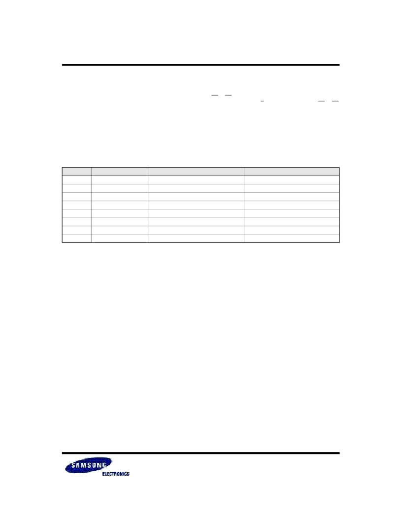
Table4. Read Staus Register Definition
NOTE
:
1. I/O 0 describes combined Pass/Fail condition for all planes. If any of the selected multiple pages/blocks fails in Program/
Erase operation, it sets "Fail" flag.
2. The pass/fail status applies only to the corresponding plane.
I/O No.
Status
Definition by 70h Command
Definition by 71h Command
I/O 0
Total Pass/Fail
Pass : "0" Fail : "1"
Pass : "0"
(1)
Fail : "1"
I/O 1
Plane 0 Pass/Fail
Must be don’t -cared
Pass : "0"
(2)
Fail : "1"
I/O 2
Plane 1 Pass/Fail
Must be don’t -cared
Pass : "0"
(2)
Fail : "1"
I/O 3
Plane 2 Pass/Fail
Must be don’t -cared
Pass : "0"
(2)
Fail : "1"
I/O 4
Plane 3 Pass/Fail
Must be don’t -cared
Pass : "0"
(2)
Fail : "1"
I/O 5
Reserved
Must be don’t -cared
Must be don’t-cared
I/O 6
Device Operation
Busy : "0" Ready : "1"
Busy : "0" Ready : "1"
I/O 7
Write Protect
Protected : "0" Not Protected : "1"
Protected : "0" Not Protected : "1"
相關(guān)PDF資料 |
PDF描述 |
|---|---|
| KBE00F005A-D411 | 512Mb NAND*2 + 256Mb Mobile SDRAM*2 |
| KBE00S003M | 1Gb NAND*2 + 256Mb Mobile SDRAM*2 |
| KBE00S003M-D411 | 1Gb NAND*2 + 256Mb Mobile SDRAM*2 |
| KBJ408G | 4.0A GLASS PASSIVATED BRIDGE RECTIFIER |
| KBJ4005G | 4.0A GLASS PASSIVATED BRIDGE RECTIFIER |
相關(guān)代理商/技術(shù)參數(shù) |
參數(shù)描述 |
|---|---|
| KBE00F005A-D411 | 制造商:SAMSUNG 制造商全稱(chēng):Samsung semiconductor 功能描述:512Mb NAND*2 + 256Mb Mobile SDRAM*2 |
| KBE00G003M | 制造商:SAMSUNG 制造商全稱(chēng):Samsung semiconductor 功能描述:NAND 512Mb*2 + Mobile SDRAM 256Mb*2 |
| KBE00G003M-D411 | 制造商:SAMSUNG 制造商全稱(chēng):Samsung semiconductor 功能描述:NAND 512Mb*2 + Mobile SDRAM 256Mb*2 |
| KBE00S003M | 制造商:SAMSUNG 制造商全稱(chēng):Samsung semiconductor 功能描述:1Gb NAND*2 + 256Mb Mobile SDRAM*2 |
| KBE00S003M-D411 | 制造商:SAMSUNG 制造商全稱(chēng):Samsung semiconductor 功能描述:1Gb NAND*2 + 256Mb Mobile SDRAM*2 |
發(fā)布緊急采購(gòu),3分鐘左右您將得到回復(fù)。