- 您現(xiàn)在的位置:買賣IC網 > PDF目錄1977 > XRT94L43IB-F (Exar Corporation)IC MAPPER SONET/SDH OC12 516BGA PDF資料下載
參數資料
| 型號: | XRT94L43IB-F |
| 廠商: | Exar Corporation |
| 文件頁數: | 71/328頁 |
| 文件大小: | 0K |
| 描述: | IC MAPPER SONET/SDH OC12 516BGA |
| 標準包裝: | 24 |
| 應用: | 網絡切換 |
| 接口: | 總線 |
| 電源電壓: | 2.5V, 3.3V |
| 封裝/外殼: | 516-BBGA |
| 供應商設備封裝: | 516-PBGA(35x35) |
| 包裝: | 托盤 |
| 安裝類型: | 表面貼裝 |
第1頁第2頁第3頁第4頁第5頁第6頁第7頁第8頁第9頁第10頁第11頁第12頁第13頁第14頁第15頁第16頁第17頁第18頁第19頁第20頁第21頁第22頁第23頁第24頁第25頁第26頁第27頁第28頁第29頁第30頁第31頁第32頁第33頁第34頁第35頁第36頁第37頁第38頁第39頁第40頁第41頁第42頁第43頁第44頁第45頁第46頁第47頁第48頁第49頁第50頁第51頁第52頁第53頁第54頁第55頁第56頁第57頁第58頁第59頁第60頁第61頁第62頁第63頁第64頁第65頁第66頁第67頁第68頁第69頁第70頁當前第71頁第72頁第73頁第74頁第75頁第76頁第77頁第78頁第79頁第80頁第81頁第82頁第83頁第84頁第85頁第86頁第87頁第88頁第89頁第90頁第91頁第92頁第93頁第94頁第95頁第96頁第97頁第98頁第99頁第100頁第101頁第102頁第103頁第104頁第105頁第106頁第107頁第108頁第109頁第110頁第111頁第112頁第113頁第114頁第115頁第116頁第117頁第118頁第119頁第120頁第121頁第122頁第123頁第124頁第125頁第126頁第127頁第128頁第129頁第130頁第131頁第132頁第133頁第134頁第135頁第136頁第137頁第138頁第139頁第140頁第141頁第142頁第143頁第144頁第145頁第146頁第147頁第148頁第149頁第150頁第151頁第152頁第153頁第154頁第155頁第156頁第157頁第158頁第159頁第160頁第161頁第162頁第163頁第164頁第165頁第166頁第167頁第168頁第169頁第170頁第171頁第172頁第173頁第174頁第175頁第176頁第177頁第178頁第179頁第180頁第181頁第182頁第183頁第184頁第185頁第186頁第187頁第188頁第189頁第190頁第191頁第192頁第193頁第194頁第195頁第196頁第197頁第198頁第199頁第200頁第201頁第202頁第203頁第204頁第205頁第206頁第207頁第208頁第209頁第210頁第211頁第212頁第213頁第214頁第215頁第216頁第217頁第218頁第219頁第220頁第221頁第222頁第223頁第224頁第225頁第226頁第227頁第228頁第229頁第230頁第231頁第232頁第233頁第234頁第235頁第236頁第237頁第238頁第239頁第240頁第241頁第242頁第243頁第244頁第245頁第246頁第247頁第248頁第249頁第250頁第251頁第252頁第253頁第254頁第255頁第256頁第257頁第258頁第259頁第260頁第261頁第262頁第263頁第264頁第265頁第266頁第267頁第268頁第269頁第270頁第271頁第272頁第273頁第274頁第275頁第276頁第277頁第278頁第279頁第280頁第281頁第282頁第283頁第284頁第285頁第286頁第287頁第288頁第289頁第290頁第291頁第292頁第293頁第294頁第295頁第296頁第297頁第298頁第299頁第300頁第301頁第302頁第303頁第304頁第305頁第306頁第307頁第308頁第309頁第310頁第311頁第312頁第313頁第314頁第315頁第316頁第317頁第318頁第319頁第320頁第321頁第322頁第323頁第324頁第325頁第326頁第327頁第328頁
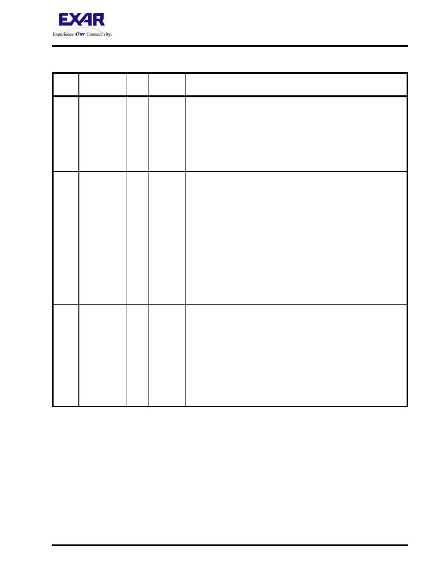
XRT94L43
156
REV. 1.0.2
SONET/SDH OC-12 TO 12XDS3/E3 MAPPER
STS-12/STM-4 TELECOM BUS INTERFACE - RECEIVE DIRECTION
PIN #
SIGNAL NAME
I/O
SIGNAL
TYPE
DESCRIPTION
V4
RxD_CLK
I
TTL
Receive STS-12/STM-4 Telecom Bus Interface - Clock Signal:
This input clock signal functions as the clock source for the Receive STS-
12/STM-4 Telecom Bus Interface. All Receive STS-12/STM-4 Telecom Bus
Interface signals are sampled upon the rising edge of this input clock sig-
nal.
This clock signal should operate at 77.76MHz.
NOTE: This input pin is only used if the STS-12/STM-4 Telecom Bus has
been enabled. It should be tied to GND otherwise.
U5
RxD_PL
I
TTL
Receive STS-12/STM-4 Telecom Bus Interface - Payload Indicator Sig-
nal:
This input pin indicates whether or not STS-1/STS-3c SPE bytes are being
input via the RXD_D[7:0] input pins.
This input pin should be pulled "High" coincident to whenever the Receive
STS-12/STM-4 Telecom Bus Interface block is receiving STS-1/STS-3c
SPE data bytes via the RXD_D[7:0] input pins.
Conversely, this input pin should be pulled "low" coincident to whenever
the Receive STS-12/STM-4 Telecom Bus Interface block is receiving
something other than an STS-1/STS-3c SPE byte (e.g., a TOH byte) via
the RXD_D[7:0] input pins.
NOTE: The user should tie this pin to GND if the STS-12/STM-4 Telecom
Bus Interface is configured to operate in the Re-Phase ON Mode
or is disabled.Tie this pin to GND if the STS-12/STM-4 Telecom
Bus is NOT enabled.
V2
RxD_C1J1
I
TTL
STS-12/STM-4 Receive Telecom Bus C1/J1 Byte Phase Indicator Input
Signal:
This input pin should be pulsed "High" during both of the following condi-
tions.
1. Whenever the C1 byte is being input to the Receive STS-12/STM-4 Tele-
com Bus Interface - Data Bus Input pins (RXD_D[7:0]).
2. Whenever the J1 byte is being input to the Receive STS-12/STM-4 Tele-
com Bus Interface - DataBus Input pins (RXD_D[7:0]).
This input pin should be pulled "low" for all other times.
NOTE:
Tie this pin to GND if the STS-12/STM-4 Telecom Bus is NOT
enabled.
相關PDF資料 |
PDF描述 |
|---|---|
| XS1-G02B-FB144-I4 | IC MCU 32BIT 16KB OTP 144FBGA |
| XTR114U/2K5 | IC 4-20MA I-TRANSMITTER 14-SOIC |
| ZXHF5000JB24TC | IC SWITCH QUAD 2X1 24QFN |
| 3341-56 | IC PLL INTEGER-N 3GHZ 20QFN |
| 3342-56 | IC PLL INTEGER-N 3GHZ 20QFN |
相關代理商/技術參數 |
參數描述 |
|---|---|
| XRT94L55 | 制造商:EXAR 制造商全稱:EXAR 功能描述:SONET/SDH OC-48/STM-16, 4XOC-12/STM-4, 16XOC-3/STM-1 FRAMER/CONCENTRATOR WITH INTEGRATED CDR’S |
| XRT94L55IV | 制造商:EXAR 制造商全稱:EXAR 功能描述:SONET/SDH OC-48/STM-16, 4XOC-12/STM-4, 16XOC-3/STM-1 FRAMER/CONCENTRATOR WITH INTEGRATED CDR’S |
| XRT95L34 | 制造商:EXAR 制造商全稱:EXAR 功能描述:OC-12/STM-4, QUAD OC-3/STM-1 POS/ATM FRAMER WITH INTEGRATED CDR’S |
| XRT95L34IV | 制造商:EXAR 制造商全稱:EXAR 功能描述:OC-12/STM-4, QUAD OC-3/STM-1 POS/ATM FRAMER WITH INTEGRATED CDR’S |
| XRT95L51 | 制造商:EXAR 制造商全稱:EXAR 功能描述:OC-48 ATM UNI/POS/MAPPER IC |
發(fā)布緊急采購,3分鐘左右您將得到回復。