- 您現(xiàn)在的位置:買賣IC網(wǎng) > PDF目錄192444 > SD-14531F5-102L (DATA DEVICE CORP) SYNCHRO OR RESOLVER TO DIGITAL CONVERTER, CDMA36 PDF資料下載
參數(shù)資料
| 型號(hào): | SD-14531F5-102L |
| 廠商: | DATA DEVICE CORP |
| 元件分類: | 位置變換器 |
| 英文描述: | SYNCHRO OR RESOLVER TO DIGITAL CONVERTER, CDMA36 |
| 封裝: | CERAMIC, FP-36 |
| 文件頁數(shù): | 13/16頁 |
| 文件大小: | 170K |
| 代理商: | SD-14531F5-102L |
6
Data Device Corporation
www.ddc-web.com
SD-14531
cos
ωt, and sin(θ+240°)cosωt are internally converted to resolver
format; sin
θcosωt and cosθcosωt.
FIGURE 3 illustrates synchro and resolver signals as a function
of the angle
θ.
The solid-state signal and reference inputs are true differential
inputs with high AC and DC common mode rejection. Input
impedance is maintained with power off.
SYNCHRO/RESOLVER PROGRAMMABLE INPUT
OPTION
The Synchro or Resolver Programmable input options are shown
in FIGURES 4 and 5.
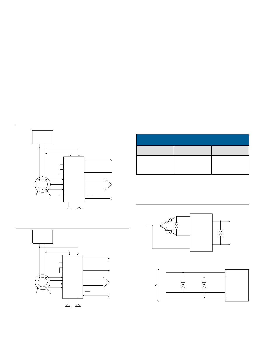
TABLE 2. COMMON-MODE AND
TRANSIENT MAXIMUMS
INPUT
COMMON-MODE
MAXIMUM
MAX. TRANSIENT
PEAK VOLTAGE
11.8 VL-L
90 VL-L
Reference
1 VL-L
30 V Peak
180 V Peak
250 V Peak
—
150 V
500 V
100 V
REFERENCE
OSCILLATOR
PARALLEL
DATA
SD-14531
STATOR
ROTOR
S3
S1
S2
S1
S3
LBE
HBE
R2
R1
LO
HI
RH
VEL (VELOCITY)
INH (INHIBIT)
CB (COUNT)
RL
S4
R
SR
S
REFERENCE
OSCILLATOR
PARALLEL
DATA
SD-14531
STATOR
ROTOR
S3
S1
S2
S1
S3
LBE
HBE
R4
R2
LO
HI
RH
VEL (VELOCITY)
INH (INHIBIT)
CB (COUNT)
RL
S4
R
SR
S
S4
FIGURE 4. SYNCHRO INPUT CONNECTION DIAGRAM
FIGURE 5. RESOLVER INPUT CONNECTION DIAGRAM
HYBRID
S3
S2
S1
RH
RL
CR1
CR2
S1
FOR 90 V SYNCHRO INPUTS
1.5kE200C
CR3
S2
S3
CR1, CR2, and CR3 are SA150CA, bipolar transient voltage suppressors
or equivalent.
HYBRID
S3
S2
S1
S4
FOR 90 V RESOLVER INPUTS
CR4
CR5
S3
S2
S1
S4
90 V L-L
RESOLVER
INPUT
CR4 and CR5 are SA150CA, bipolar transient voltage suppressors or equivalent.
FIGURE 6. CONNECTIONS FOR VOLTAGE
TRANSIENT SUPPRESSORS
SOLID-STATE BUFFER INPUT PROTECTION —
TRANSIENT VOLTAGE SUPPRESSION
The solid-state signal and reference inputs are true differential
inputs with high AC and DC common rejection, so most applica-
tions will not require units with isolation transformers. Input imped-
ance is maintained with power off. The recurrent AC peak + DC
common-mode voltage should not exceed the values in TABLE 2.
The 90 V line-to-line systems may have voltage transients which
exceed the 500 V specification listed in TABLE 2. These tran-
sients can destroy the thin-film input resistor network in the
hybrid. Therefore, 90 V L-L solid-state input modules may be pro-
tected by installing voltage suppressors as shown. Voltage tran-
sients are likely to occur whenever synchro or resolver are
switched on and off. For instance a 1000 V transient can be gen-
erated when the primary of a CX or TX driving a synchro or
resolver input is opened (see FIGURE 6).
相關(guān)PDF資料 |
PDF描述 |
|---|---|
| SD-14531F5-102Q | SYNCHRO OR RESOLVER TO DIGITAL CONVERTER, CDMA36 |
| SD-14531F5-102S | SYNCHRO OR RESOLVER TO DIGITAL CONVERTER, CDMA36 |
| SD-14531F5-102Z | SYNCHRO OR RESOLVER TO DIGITAL CONVERTER, CDMA36 |
| SD-14531F5-105Y | SYNCHRO OR RESOLVER TO DIGITAL CONVERTER, CDMA36 |
| SD-14531F5-202K | SYNCHRO OR RESOLVER TO DIGITAL CONVERTER, CDMA36 |
相關(guān)代理商/技術(shù)參數(shù) |
參數(shù)描述 |
|---|---|
| SD1455 | 功能描述:射頻雙極電源晶體管 NPN 25V 170-230MHz RoHS:否 制造商:M/A-COM Technology Solutions 配置:Single 直流集電極/Base Gain hfe Min:40 最大工作頻率:30 MHz 集電極—發(fā)射極最大電壓 VCEO:25 V 發(fā)射極 - 基極電壓 VEBO:4 V 集電極連續(xù)電流:20 A 最大直流電集電極電流: 功率耗散:250 W 封裝 / 箱體:Case 211-11 封裝:Tray |
| SD1456 | 功能描述:射頻雙極電源晶體管 NPN 28V 170-230MHz RoHS:否 制造商:M/A-COM Technology Solutions 配置:Single 直流集電極/Base Gain hfe Min:40 最大工作頻率:30 MHz 集電極—發(fā)射極最大電壓 VCEO:25 V 發(fā)射極 - 基極電壓 VEBO:4 V 集電極連續(xù)電流:20 A 最大直流電集電極電流: 功率耗散:250 W 封裝 / 箱體:Case 211-11 封裝:Tray |
| SD1457 | 功能描述:射頻放大器 RF Bipolar Trans RoHS:否 制造商:Skyworks Solutions, Inc. 類型:Low Noise Amplifier 工作頻率:2.3 GHz to 2.8 GHz P1dB:18.5 dBm 輸出截獲點(diǎn):37.5 dBm 功率增益類型:32 dB 噪聲系數(shù):0.85 dB 工作電源電壓:5 V 電源電流:125 mA 測試頻率:2.6 GHz 最大工作溫度:+ 85 C 安裝風(fēng)格:SMD/SMT 封裝 / 箱體:QFN-16 封裝:Reel |
| SD1458 | 功能描述:射頻放大器 RF Bipolar Trans RoHS:否 制造商:Skyworks Solutions, Inc. 類型:Low Noise Amplifier 工作頻率:2.3 GHz to 2.8 GHz P1dB:18.5 dBm 輸出截獲點(diǎn):37.5 dBm 功率增益類型:32 dB 噪聲系數(shù):0.85 dB 工作電源電壓:5 V 電源電流:125 mA 測試頻率:2.6 GHz 最大工作溫度:+ 85 C 安裝風(fēng)格:SMD/SMT 封裝 / 箱體:QFN-16 封裝:Reel |
| SD1459 | 功能描述:射頻雙極電源晶體管 NPN 28V 170-230MHz RoHS:否 制造商:M/A-COM Technology Solutions 配置:Single 直流集電極/Base Gain hfe Min:40 最大工作頻率:30 MHz 集電極—發(fā)射極最大電壓 VCEO:25 V 發(fā)射極 - 基極電壓 VEBO:4 V 集電極連續(xù)電流:20 A 最大直流電集電極電流: 功率耗散:250 W 封裝 / 箱體:Case 211-11 封裝:Tray |
發(fā)布緊急采購,3分鐘左右您將得到回復(fù)。