- 您現(xiàn)在的位置:買賣IC網(wǎng) > PDF目錄384797 > OR4E6 (Lineage Power) Field-Programmable Gate Arrays(現(xiàn)場可編程門陣列) PDF資料下載
參數(shù)資料
| 型號: | OR4E6 |
| 廠商: | Lineage Power |
| 英文描述: | Field-Programmable Gate Arrays(現(xiàn)場可編程門陣列) |
| 中文描述: | 現(xiàn)場可編程門陣列(現(xiàn)場可編程門陣列) |
| 文件頁數(shù): | 71/132頁 |
| 文件大小: | 2667K |
| 代理商: | OR4E6 |
第1頁第2頁第3頁第4頁第5頁第6頁第7頁第8頁第9頁第10頁第11頁第12頁第13頁第14頁第15頁第16頁第17頁第18頁第19頁第20頁第21頁第22頁第23頁第24頁第25頁第26頁第27頁第28頁第29頁第30頁第31頁第32頁第33頁第34頁第35頁第36頁第37頁第38頁第39頁第40頁第41頁第42頁第43頁第44頁第45頁第46頁第47頁第48頁第49頁第50頁第51頁第52頁第53頁第54頁第55頁第56頁第57頁第58頁第59頁第60頁第61頁第62頁第63頁第64頁第65頁第66頁第67頁第68頁第69頁第70頁當(dāng)前第71頁第72頁第73頁第74頁第75頁第76頁第77頁第78頁第79頁第80頁第81頁第82頁第83頁第84頁第85頁第86頁第87頁第88頁第89頁第90頁第91頁第92頁第93頁第94頁第95頁第96頁第97頁第98頁第99頁第100頁第101頁第102頁第103頁第104頁第105頁第106頁第107頁第108頁第109頁第110頁第111頁第112頁第113頁第114頁第115頁第116頁第117頁第118頁第119頁第120頁第121頁第122頁第123頁第124頁第125頁第126頁第127頁第128頁第129頁第130頁第131頁第132頁
Lucent Technologies Inc.
71
Preliminary Data Sheet
August 2000
ORCA Series 4 FPGAs
FPGA Configuration Modes
(continued)
5-4487(F)
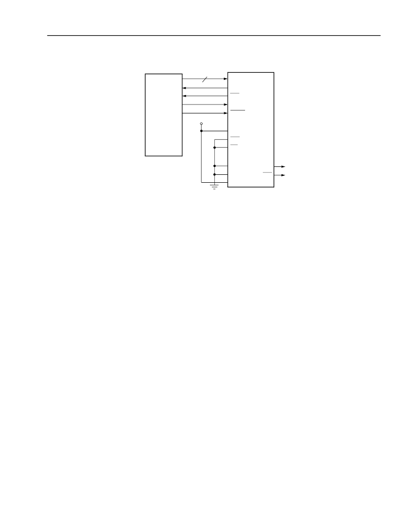
Figure 45. Slave Parallel Configuration Schematic
Daisy Chaining
Multiple FPGAs can be configured by using a daisy chain of the FPGAs. Daisy chaining uses a lead FPGA and one
or more FPGAs configured in slave serial mode. The lead FPGA can be configured in any mode except slave paral-
lel mode. (Daisy chaining is available with the boundary-scan ram_w instruction discussed later.)
All daisy-chained FPGAs are connected in series. Each FPGA reads and shifts the preamble and length count in on
positive CCLK and out on negative CCLK edges.
An upstream FPGA that has received the preamble and length count outputs a high on DOUT until it has received
the appropriate number of data frames so that downstream FPGAs do not receive frame start bit pairs. After loading
and retransmitting the preamble and length count to a daisy chain of slave devices, the lead device loads its config-
uration data frames. The loading of configuration data continues after the lead device has received its configuration
data if its internal frame bit counter has not reached the length count. When the configuration RAM is full and the
number of bits received is less than the length count field, the FPGA shifts any additional data out on DOUT.
The configuration data is read into DIN of slave devices on the positive edge of CCLK, and shifted out DOUT on the
negative edge of CCLK. Figure 46 shows the connections for loading multiple FPGAs in a daisy-chain configura-
tion.
The generation of CCLK for the daisy-chained devices that are in slave serial mode differs depending on the config-
uration mode of the lead device. A master parallel mode device uses its internal timing generator to produce an
internal CCLK at eight times its memory address rate (RCLK). The asynchronous peripheral mode device outputs
eight CCLKs for each write cycle. If the lead device is configured in slave mode, CCLK must be routed to the lead
device and to all of the daisy-chained devices.
MICRO-
PROCESSOR
OR
SYSTEM
D[7:0]
DONE
INIT
CCLK
CS1
CS0
WR
M2
M1
M0
HDC
LDC
8
V
DD
PRGM
ORCA
FPGA
相關(guān)PDF資料 |
PDF描述 |
|---|---|
| ORT4622 | Field-Programmable System Chip (FPSC) Four Channel x 622 Mbits/s Backplane Transceiver(現(xiàn)場可編程系統(tǒng)芯片(四通道x 622 M位/秒背板收發(fā)器)) |
| ORT8850 | Field-Programmable System Chip(現(xiàn)場可編程系統(tǒng)芯片) |
| OS8740230 | Si Optical Receiver, 40 - 870MHz, 225mA max. @ 24VDC |
| OSC-1A0 | Ultra Miniature TCXO |
| OSC-1A1 | Ultra Miniature TCXO |
相關(guān)代理商/技術(shù)參數(shù) |
參數(shù)描述 |
|---|---|
| OR4E6-1BA352 | 制造商:未知廠家 制造商全稱:未知廠家 功能描述:FPGA |
| OR4E6-1BC432 | 制造商:未知廠家 制造商全稱:未知廠家 功能描述:FPGA |
| OR4E6-1BM680 | 制造商:未知廠家 制造商全稱:未知廠家 功能描述:FPGA |
| OR4E6-2BA352 | 制造商:未知廠家 制造商全稱:未知廠家 功能描述:FPGA |
| OR4E6-2BC432 | 制造商:未知廠家 制造商全稱:未知廠家 功能描述:FPGA |
發(fā)布緊急采購,3分鐘左右您將得到回復(fù)。