- 您現(xiàn)在的位置:買賣IC網(wǎng) > PDF目錄384797 > OR4E6 (Lineage Power) Field-Programmable Gate Arrays(現(xiàn)場(chǎng)可編程門陣列) PDF資料下載
參數(shù)資料
| 型號(hào): | OR4E6 |
| 廠商: | Lineage Power |
| 英文描述: | Field-Programmable Gate Arrays(現(xiàn)場(chǎng)可編程門陣列) |
| 中文描述: | 現(xiàn)場(chǎng)可編程門陣列(現(xiàn)場(chǎng)可編程門陣列) |
| 文件頁數(shù): | 52/132頁 |
| 文件大小: | 2667K |
| 代理商: | OR4E6 |
第1頁第2頁第3頁第4頁第5頁第6頁第7頁第8頁第9頁第10頁第11頁第12頁第13頁第14頁第15頁第16頁第17頁第18頁第19頁第20頁第21頁第22頁第23頁第24頁第25頁第26頁第27頁第28頁第29頁第30頁第31頁第32頁第33頁第34頁第35頁第36頁第37頁第38頁第39頁第40頁第41頁第42頁第43頁第44頁第45頁第46頁第47頁第48頁第49頁第50頁第51頁當(dāng)前第52頁第53頁第54頁第55頁第56頁第57頁第58頁第59頁第60頁第61頁第62頁第63頁第64頁第65頁第66頁第67頁第68頁第69頁第70頁第71頁第72頁第73頁第74頁第75頁第76頁第77頁第78頁第79頁第80頁第81頁第82頁第83頁第84頁第85頁第86頁第87頁第88頁第89頁第90頁第91頁第92頁第93頁第94頁第95頁第96頁第97頁第98頁第99頁第100頁第101頁第102頁第103頁第104頁第105頁第106頁第107頁第108頁第109頁第110頁第111頁第112頁第113頁第114頁第115頁第116頁第117頁第118頁第119頁第120頁第121頁第122頁第123頁第124頁第125頁第126頁第127頁第128頁第129頁第130頁第131頁第132頁
52
Lucent Technologies Inc.
Preliminary Data Sheet
August 2000
ORCA Series 4 FPGAs
Phase-Locked Loops
There are eight PLLs available to perform many clock
modification and clock conditioning functions on the
Series 4 FPGAs. Six of the PLLs are programmable
allowing the user the flexibility to configure the PLL to
manipulate the frequency, phase, and duty cycle of a
clock signal. Four of the programmable PLLs are capa-
ble of manipulating and conditioning clocks from
20 MHz to 200 MHz and two others are capable of
manipulating and conditioning clocks from 60 MHz to
420 MHz. Frequencies can be adjusted from 1/8x to 8x
the input clock frequency. Each programmable PLL
provides two outputs that have different multiplication
factors with the same phase relationships. Duty cycles
and phase delays can be adjusted in 12.5% of the
clock period increments. An input buffer delay compen-
sation mode is available for phase delay. Each PPLL
provides two outputs (MCLK, NCLK) that can have pro-
grammable (12.5% steps) phase differences.
The PPLLs can be utilized to eliminate skew between
the clock input pad and the internal clock inputs across
the entire device. The PPLLs can drive onto the pri-
mary, secondary, and edge clock networks inside the
FPGA. Each PPLL can take a clock input from the ded-
icated pad or differential pair of pads in its corner or
from general routing resources.
Functionality of the PPLLs is programmed during oper-
ation through a read/write interface to the internal sys-
tem bus command and status registers or via the
configuration bit stream. There is also a PLL output sig-
nal, LOCK, that indicates a stable output clock state.
Unlike Series 3, this signal does not have to be inter-
grated before use.
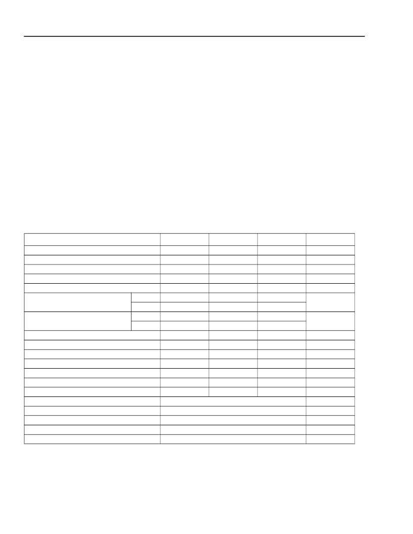
Table 31. PPLL Specifications
Additional highly tuned and characterized dedicated phase-locked loops (DPLLs) are included to ease system
designs. These DPLLs meet ITU-T G.811 primary clocking specifications and enable system designers to target
very tightly specified clock conditioning not available in the universal PPLLs. DPLLs are targeted to low-speed net-
working DS1 and E1 and high-speed SONET/SDH networking STS-3 and STM-1 systems.
Parameter
Min
1.425
3.0
–40
1.425
1.425
20
60
20
60
30
45
—
—
—
—
—
Nom
1.5
3.3
25
1.5
1.5
—
—
—
—
—
50
28
8.5
30
<0.02
<50
Max
1.575
3.6
125
1.575
1.575
200
420
200
420
70
55
—
—
—
—
—
Unit
V
V
°C
V
V
MHz
V
DD
1.5
V
DD
3.3
Operating Temp
Input Clock Voltage
Output Clock Voltage
Input Clock Frequency
(no division)
Output Clock Frequency
PPLL
HPPLL
PPLL
HPPLL
MHz
Input Duty Cycle Tolerance
Output Duty Cycle
dc Power
Total On Current
Total Off Current
Cycle to Cycle Jitter (p-p)
Lock Time
Frequency Multiplication
Frequency Division
Duty Cycle Adjust of Output Clock
Delay Adjust of Output Clock
Phase Shift Between MCLK & NCLK
%
%
mW
mA
pA
UIp-p
μs
—
—
%
%
degree
1x, 2x, 3x, 4x, 5x, 6x, 7x, 8x,
1/8, 1/7, 1/6, 1/5, 1/4, 1/3, 1/2
12.5, 25, 37.5, 50, 62.5, 75, 87.5
0, 12.5, 25, 37.5, 50, 62.5, 75, 87.5
0, 45, 90, 135, 180, 225, 270, 315
相關(guān)PDF資料 |
PDF描述 |
|---|---|
| ORT4622 | Field-Programmable System Chip (FPSC) Four Channel x 622 Mbits/s Backplane Transceiver(現(xiàn)場(chǎng)可編程系統(tǒng)芯片(四通道x 622 M位/秒背板收發(fā)器)) |
| ORT8850 | Field-Programmable System Chip(現(xiàn)場(chǎng)可編程系統(tǒng)芯片) |
| OS8740230 | Si Optical Receiver, 40 - 870MHz, 225mA max. @ 24VDC |
| OSC-1A0 | Ultra Miniature TCXO |
| OSC-1A1 | Ultra Miniature TCXO |
相關(guān)代理商/技術(shù)參數(shù) |
參數(shù)描述 |
|---|---|
| OR4E6-1BA352 | 制造商:未知廠家 制造商全稱:未知廠家 功能描述:FPGA |
| OR4E6-1BC432 | 制造商:未知廠家 制造商全稱:未知廠家 功能描述:FPGA |
| OR4E6-1BM680 | 制造商:未知廠家 制造商全稱:未知廠家 功能描述:FPGA |
| OR4E6-2BA352 | 制造商:未知廠家 制造商全稱:未知廠家 功能描述:FPGA |
| OR4E6-2BC432 | 制造商:未知廠家 制造商全稱:未知廠家 功能描述:FPGA |
發(fā)布緊急采購,3分鐘左右您將得到回復(fù)。