- 您現(xiàn)在的位置:買賣IC網(wǎng) > PDF目錄384797 > OR4E6 (Lineage Power) Field-Programmable Gate Arrays(現(xiàn)場可編程門陣列) PDF資料下載
參數(shù)資料
| 型號(hào): | OR4E6 |
| 廠商: | Lineage Power |
| 英文描述: | Field-Programmable Gate Arrays(現(xiàn)場可編程門陣列) |
| 中文描述: | 現(xiàn)場可編程門陣列(現(xiàn)場可編程門陣列) |
| 文件頁數(shù): | 70/132頁 |
| 文件大小: | 2667K |
| 代理商: | OR4E6 |
第1頁第2頁第3頁第4頁第5頁第6頁第7頁第8頁第9頁第10頁第11頁第12頁第13頁第14頁第15頁第16頁第17頁第18頁第19頁第20頁第21頁第22頁第23頁第24頁第25頁第26頁第27頁第28頁第29頁第30頁第31頁第32頁第33頁第34頁第35頁第36頁第37頁第38頁第39頁第40頁第41頁第42頁第43頁第44頁第45頁第46頁第47頁第48頁第49頁第50頁第51頁第52頁第53頁第54頁第55頁第56頁第57頁第58頁第59頁第60頁第61頁第62頁第63頁第64頁第65頁第66頁第67頁第68頁第69頁當(dāng)前第70頁第71頁第72頁第73頁第74頁第75頁第76頁第77頁第78頁第79頁第80頁第81頁第82頁第83頁第84頁第85頁第86頁第87頁第88頁第89頁第90頁第91頁第92頁第93頁第94頁第95頁第96頁第97頁第98頁第99頁第100頁第101頁第102頁第103頁第104頁第105頁第106頁第107頁第108頁第109頁第110頁第111頁第112頁第113頁第114頁第115頁第116頁第117頁第118頁第119頁第120頁第121頁第122頁第123頁第124頁第125頁第126頁第127頁第128頁第129頁第130頁第131頁第132頁
70
Lucent Technologies Inc.
Preliminary Data Sheet
August 2000
ORCA Series 4 FPGAs
FPGA Configuration Modes
(continued)
Slave Serial Mode
The slave serial mode is primarily used when multiple FPGAs are configured in a daisy-chain (see the Daisy
Chaining section). It is also used on the FPGA evaluation board that interfaces to the download cable. A device in
the slave serial mode can be used as the lead device in a daisy chain. Figure 44 shows the connections for the
slave serial configuration mode.
The configuration data is provided into the FPGA’s DIN input synchronous with the configuration clock CCLK input.
After the FPGA has loaded its configuration data, it retransmits the incoming configuration data on DOUT. CCLK is
routed into all slave serial mode devices in parallel.
Multiple slave FPGAs can be loaded with identical configurations simultaneously. This is done by loading the con-
figuration data into the DIN inputs in parallel.
5-4485(F)
Figure 44. Slave Serial Configuration Schematic
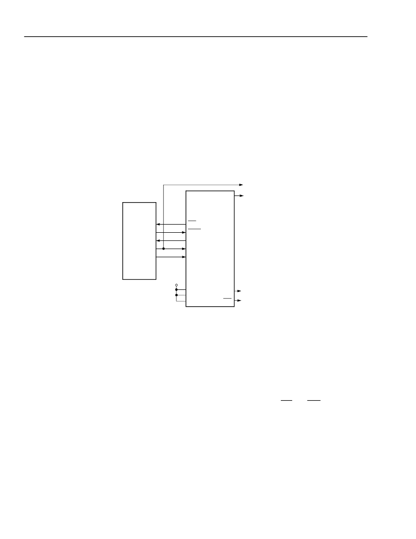
Slave Parallel Mode
The slave parallel mode is essentially the same as the slave serial mode except that 8 bits of data are input on pins
D[7:0] for each CCLK cycle. Due to 8 bits of data being input per CCLK cycle, the DOUT pin does not contain a
valid bit stream for slave parallel mode. As a result, the lead device cannot be used in the slave parallel mode in a
daisy-chain configuration.
Figure 45
is a schematic of the connections for the slave parallel configuration mode. WR and CS0 are active-low
chip select signals, and CS1 is an active-high chip select signal. These chip selects allow the user to configure mul-
tiple FPGAs in slave parallel mode using an 8-bit data bus common to all of the FPGAs. These chip selects can
then be used to select the FPGAs to be configured with a given bit stream. The chip selects must be active for each
valid CCLK cycle until the device has been completely programmed. They can be inactive between cycles but must
meet the setup and hold times for each valid positive CCLK. D[7:0] of the FPGA can be connected to D[7:0] of the
microprocessor only if a standard prom file format is used. If a .bit or .rbt file is used from ORCA Foundry, then the
user must mirror the bytes in the .bit or .rbt file
or
leave the .bit or .rbt file unchanged and connect D[7:0] of the
FPGA to D[0:7] of the microprocessor.
MICRO-
PROCESSOR
OR
DOWNLOAD
CABLE
M2
M1
M0
HDC
ORCA
FPGA
LDC
V
DD
CCLK
PRGM
DOUT
TO DAISY-
CHAINED
DEVICES
DONE
DIN
INIT
相關(guān)PDF資料 |
PDF描述 |
|---|---|
| ORT4622 | Field-Programmable System Chip (FPSC) Four Channel x 622 Mbits/s Backplane Transceiver(現(xiàn)場可編程系統(tǒng)芯片(四通道x 622 M位/秒背板收發(fā)器)) |
| ORT8850 | Field-Programmable System Chip(現(xiàn)場可編程系統(tǒng)芯片) |
| OS8740230 | Si Optical Receiver, 40 - 870MHz, 225mA max. @ 24VDC |
| OSC-1A0 | Ultra Miniature TCXO |
| OSC-1A1 | Ultra Miniature TCXO |
相關(guān)代理商/技術(shù)參數(shù) |
參數(shù)描述 |
|---|---|
| OR4E6-1BA352 | 制造商:未知廠家 制造商全稱:未知廠家 功能描述:FPGA |
| OR4E6-1BC432 | 制造商:未知廠家 制造商全稱:未知廠家 功能描述:FPGA |
| OR4E6-1BM680 | 制造商:未知廠家 制造商全稱:未知廠家 功能描述:FPGA |
| OR4E6-2BA352 | 制造商:未知廠家 制造商全稱:未知廠家 功能描述:FPGA |
| OR4E6-2BC432 | 制造商:未知廠家 制造商全稱:未知廠家 功能描述:FPGA |
發(fā)布緊急采購,3分鐘左右您將得到回復(fù)。