- 您現(xiàn)在的位置:買賣IC網(wǎng) > PDF目錄384755 > MT28F160S3 (Micron Technology, Inc.) 2 Meg x 8/1 Meg x 16 Smart 3 Flash(2 M x 8/1 M x 16閃速存儲器) PDF資料下載
參數(shù)資料
| 型號: | MT28F160S3 |
| 廠商: | Micron Technology, Inc. |
| 英文描述: | 2 Meg x 8/1 Meg x 16 Smart 3 Flash(2 M x 8/1 M x 16閃速存儲器) |
| 中文描述: | 2梅格× 8 /檢測起× 16智能3閃光(2 M中的x 8月1日M中的x 16閃速存儲器) |
| 文件頁數(shù): | 21/39頁 |
| 文件大小: | 281K |
| 代理商: | MT28F160S3 |
第1頁第2頁第3頁第4頁第5頁第6頁第7頁第8頁第9頁第10頁第11頁第12頁第13頁第14頁第15頁第16頁第17頁第18頁第19頁第20頁當前第21頁第22頁第23頁第24頁第25頁第26頁第27頁第28頁第29頁第30頁第31頁第32頁第33頁第34頁第35頁第36頁第37頁第38頁第39頁
21
2 Meg x 8 /1 Meg x 16 Even-Sectored Flash Memory
MT28F160S3_2 – Rev. 8/00
Micron Technology, Inc., reserves the right to change products or specifications without notice.
2000, Micron Technology, Inc.
2 MEG x 8/1 MEG x 16
SMART 3 EVEN-SECTORED FLASH
PRELIMINARY
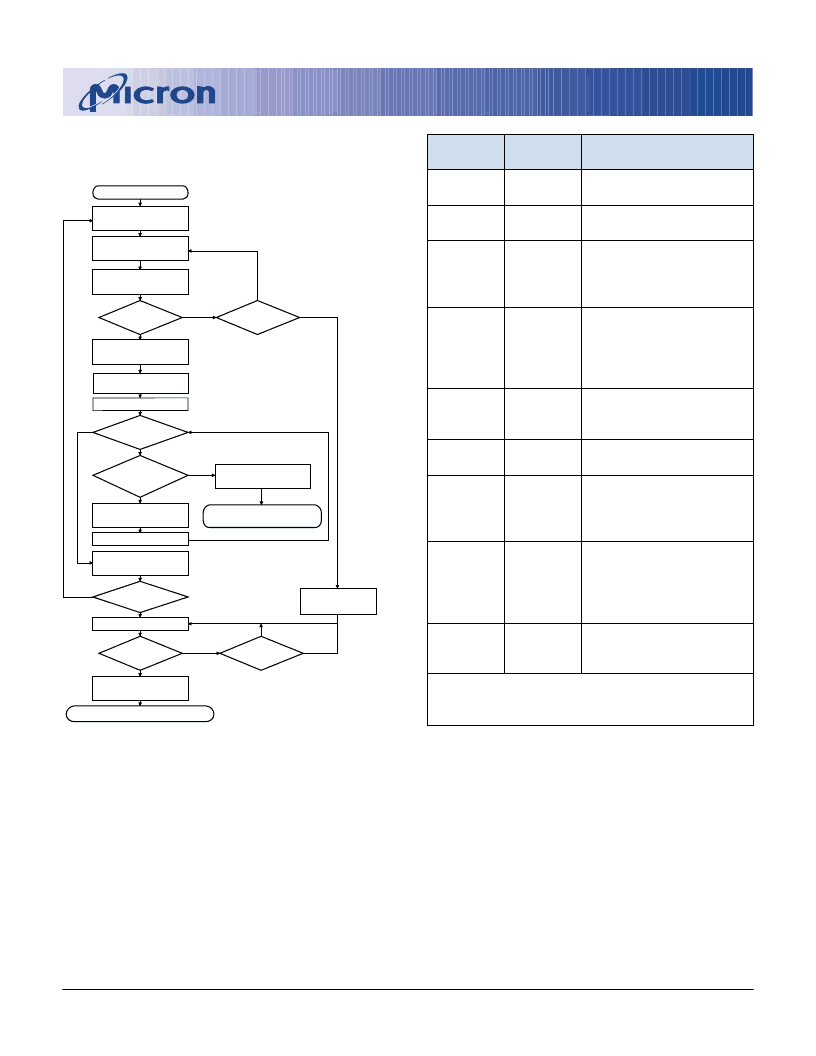
Figure 3
WRITE-to-BUFFER Flowchart
YES
NO
NO
NO
YES
Set Timeout
Start
0
1
NO
Read Extended
Status Register
Issue WRITE Command
Eh8, Block Address
XR7=
Write Buffer
Timeout
Write Word or Byte
Count, Block Address
Write Buffer Data
Start Address
X = 0
Check
X = N
Abort
BUFFER WRITE
Command
Write to Another
Block Address
BUFFER
WRITE-to-
Flash Aborted
NO
Write Next Buffer
Data, Device Address
X = X + 1
BUFFER WRITE-to-Flash
Confirm D0h
Another
BUFFER WRITE
Read Status Register
SR7=
BUFFER WRITE-to-Flash Complete
Suspend Write
Issue READ
STATUS Command
0
YES
Suspend
Write Loop
1
YES
Full Status Check
if Desired
BUS
OPERATION COMMAND COMMENTS
WRITE
WRITE-to-
BUFFER
READ
Data = E8h
Block Address
XSR 7 = Valid
Addr = X
Check XSR 7
1 = Write Buffer Available
0 = Write Buffer Not
Available
Data = N = Word/Byte
Count
N = 0 Corresponds to
Count = 1
Addr = Block Address
Data = Write Buffer Data
Addr = Device Start
Address
Data = Write Buffer Data
Addr = Device Address
Data = D0h
Addr = X
STANDBY
WRITE
1,2
WRITE
3,4
WRITE
5,6
WRITE
BUFFER
WRITE-to-
FLASH
CONFIRM
READ
Status register data with
the device enabled, OE#
LOW
Updates SR
Addr = X
Check SR7
1 = ISM Ready
0 = ISM Busy
STANDBY
Full status check can be done after all erase and
write sequences complete. Write FFh after the last
operation to reset the device to read array mode.
NOTE:
1. Byte or word count values on DQ0-DQ7 are loaded into the count register. Count ranges on this device for byte mode
are N = 00h to 1Fh and for word mode are N = 0000h to 000Fh.
2. The device now outputs the status register when read (XSR is no longer available).
3. Write buffer contents will be programmed at the device start address or destination flash address.
4. Align the start address on a write buffer boundary for maximum programming performance (i.e., A4-A0 of the start
address = 0).
5. The device aborts the WRITE-to-BUFFER command if the current address is outside of the original block address.
6. The status register indicates an “ improper command sequence” if the WRITE-to-BUFFER command is aborted. Follow
this with a CLEAR STATUS REGISTER command.
相關PDF資料 |
PDF描述 |
|---|---|
| MT28F640J3 | 64Mb Flash Memory(64Mb閃速存儲器) |
| MT35212A | BELL 212A/CCITT V.22 Modem Filter |
| MT35212AE | BELL 212A/CCITT V.22 Modem Filter |
| MT35212AP | BELL 212A/CCITT V.22 Modem Filter |
| MT46V32M16TG-8L | DOUBLE DATA RATE DDR SDRAM |
相關代理商/技術參數(shù) |
參數(shù)描述 |
|---|---|
| MT28F200B3 | 制造商:MICRON 制造商全稱:Micron Technology 功能描述:FLASH MEMORY |
| MT28F200B5 | 制造商:MICRON 制造商全稱:Micron Technology 功能描述:FLASH MEMORY |
| MT28F200B5SG-6 B | 制造商:Micron Technology Inc 功能描述:NOR Flash Parallel 5V 2Mbit 256K/128K x 8bit/16bit 60ns 44-Pin SOP Tray |
| MT28F200B5SG-6 T | 制造商:Micron Technology Inc 功能描述:NOR Flash Parallel 5V 2Mbit 256K/128K x 8bit/16bit 60ns 44-Pin SOP Tray |
| MT28F200B5SG-8 B TR | 制造商:Micron Technology Inc 功能描述:Flash Mem Parallel 5V 2M-Bit 256K x 8/128K x 16 80ns 44-Pin SOP T/R |
發(fā)布緊急采購,3分鐘左右您將得到回復。