- 您現(xiàn)在的位置:買賣IC網(wǎng) > PDF目錄371051 > MC68HC11KW1 (MOTOROLA INC) High-density complementary metal oxide semiconductor HCMOS) microcontroller unit PDF資料下載
參數(shù)資料
| 型號(hào): | MC68HC11KW1 |
| 廠商: | MOTOROLA INC |
| 元件分類: | 微控制器/微處理器 |
| 英文描述: | High-density complementary metal oxide semiconductor HCMOS) microcontroller unit |
| 中文描述: | 8-BIT, EEPROM, 4 MHz, MICROCONTROLLER, PQFP100 |
| 封裝: | TQFP-100 |
| 文件頁(yè)數(shù): | 159/238頁(yè) |
| 文件大小: | 798K |
| 代理商: | MC68HC11KW1 |
第1頁(yè)第2頁(yè)第3頁(yè)第4頁(yè)第5頁(yè)第6頁(yè)第7頁(yè)第8頁(yè)第9頁(yè)第10頁(yè)第11頁(yè)第12頁(yè)第13頁(yè)第14頁(yè)第15頁(yè)第16頁(yè)第17頁(yè)第18頁(yè)第19頁(yè)第20頁(yè)第21頁(yè)第22頁(yè)第23頁(yè)第24頁(yè)第25頁(yè)第26頁(yè)第27頁(yè)第28頁(yè)第29頁(yè)第30頁(yè)第31頁(yè)第32頁(yè)第33頁(yè)第34頁(yè)第35頁(yè)第36頁(yè)第37頁(yè)第38頁(yè)第39頁(yè)第40頁(yè)第41頁(yè)第42頁(yè)第43頁(yè)第44頁(yè)第45頁(yè)第46頁(yè)第47頁(yè)第48頁(yè)第49頁(yè)第50頁(yè)第51頁(yè)第52頁(yè)第53頁(yè)第54頁(yè)第55頁(yè)第56頁(yè)第57頁(yè)第58頁(yè)第59頁(yè)第60頁(yè)第61頁(yè)第62頁(yè)第63頁(yè)第64頁(yè)第65頁(yè)第66頁(yè)第67頁(yè)第68頁(yè)第69頁(yè)第70頁(yè)第71頁(yè)第72頁(yè)第73頁(yè)第74頁(yè)第75頁(yè)第76頁(yè)第77頁(yè)第78頁(yè)第79頁(yè)第80頁(yè)第81頁(yè)第82頁(yè)第83頁(yè)第84頁(yè)第85頁(yè)第86頁(yè)第87頁(yè)第88頁(yè)第89頁(yè)第90頁(yè)第91頁(yè)第92頁(yè)第93頁(yè)第94頁(yè)第95頁(yè)第96頁(yè)第97頁(yè)第98頁(yè)第99頁(yè)第100頁(yè)第101頁(yè)第102頁(yè)第103頁(yè)第104頁(yè)第105頁(yè)第106頁(yè)第107頁(yè)第108頁(yè)第109頁(yè)第110頁(yè)第111頁(yè)第112頁(yè)第113頁(yè)第114頁(yè)第115頁(yè)第116頁(yè)第117頁(yè)第118頁(yè)第119頁(yè)第120頁(yè)第121頁(yè)第122頁(yè)第123頁(yè)第124頁(yè)第125頁(yè)第126頁(yè)第127頁(yè)第128頁(yè)第129頁(yè)第130頁(yè)第131頁(yè)第132頁(yè)第133頁(yè)第134頁(yè)第135頁(yè)第136頁(yè)第137頁(yè)第138頁(yè)第139頁(yè)第140頁(yè)第141頁(yè)第142頁(yè)第143頁(yè)第144頁(yè)第145頁(yè)第146頁(yè)第147頁(yè)第148頁(yè)第149頁(yè)第150頁(yè)第151頁(yè)第152頁(yè)第153頁(yè)第154頁(yè)第155頁(yè)第156頁(yè)第157頁(yè)第158頁(yè)當(dāng)前第159頁(yè)第160頁(yè)第161頁(yè)第162頁(yè)第163頁(yè)第164頁(yè)第165頁(yè)第166頁(yè)第167頁(yè)第168頁(yè)第169頁(yè)第170頁(yè)第171頁(yè)第172頁(yè)第173頁(yè)第174頁(yè)第175頁(yè)第176頁(yè)第177頁(yè)第178頁(yè)第179頁(yè)第180頁(yè)第181頁(yè)第182頁(yè)第183頁(yè)第184頁(yè)第185頁(yè)第186頁(yè)第187頁(yè)第188頁(yè)第189頁(yè)第190頁(yè)第191頁(yè)第192頁(yè)第193頁(yè)第194頁(yè)第195頁(yè)第196頁(yè)第197頁(yè)第198頁(yè)第199頁(yè)第200頁(yè)第201頁(yè)第202頁(yè)第203頁(yè)第204頁(yè)第205頁(yè)第206頁(yè)第207頁(yè)第208頁(yè)第209頁(yè)第210頁(yè)第211頁(yè)第212頁(yè)第213頁(yè)第214頁(yè)第215頁(yè)第216頁(yè)第217頁(yè)第218頁(yè)第219頁(yè)第220頁(yè)第221頁(yè)第222頁(yè)第223頁(yè)第224頁(yè)第225頁(yè)第226頁(yè)第227頁(yè)第228頁(yè)第229頁(yè)第230頁(yè)第231頁(yè)第232頁(yè)第233頁(yè)第234頁(yè)第235頁(yè)第236頁(yè)第237頁(yè)第238頁(yè)
MC68HC11KW1
MOTOROLA
9-7
TIMING SYSTEM
9
9.1.2.2
TIC1–TIC3 — Timer input capture registers
When an edge has been detected and synchronized, the 16-bit free-running counter value is
transferred into the input capture register pair as a single 16-bit parallel transfer. Timer counter
value captures and timer counter incrementing occur on opposite half-cycles of the phase 2 clock
so that the count value is stable whenever a capture occurs. Input capture values can be read from
a pair of 8-bit read-only registers. A read of the high-order byte of an input capture register pair
inhibits a new capture transfer for one bus cycle. If a double-byte read instruction, such as LDD,
is used to read the captured value, coherency is assured. When a new input capture occurs
immediately after a high-order byte read, transfer is delayed for an additional cycle but the value
is not lost.
The TICx registers are not affected by reset.
9.1.2.3
TI4/O5 — Timer input capture 4/output compare 5
register
Use TI4/O5 as either an input capture register or an output compare register, depending on the
function chosen for the PA3 pin. To enable it as an input capture pin, set the I4/O5 bit in the pulse
accumulator control register (PACTL) to logic level one. To use it as an output compare register,
set the I4/O5 bit to a logic level zero. Refer to Section 9.6.1.
The TI4/O5 register pair resets to ones ($FFFF).
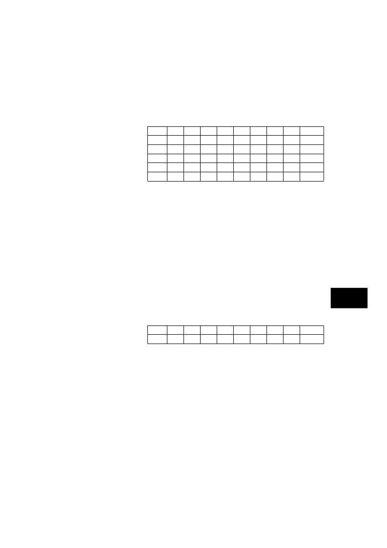
Address
bit 7
bit 6
bit 5
bit 4
bit 3
bit 2
bit 1
bit 0
State
on reset
Timer input capture 1 (TIC1) high
$0010
(bit 15)
(14)
(13)
(12)
(11)
(10)
(9)
(bit 8) not affected
Timer input capture 1 (TIC1) low
$0011
(bit 7)
(6)
(5)
(4)
(3)
(2)
(1)
(bit 0) not affected
Timer input capture 2 (TIC2) high
$0012
(bit 15)
(14)
(13)
(12)
(11)
(10)
(9)
(bit 8) not affected
Timer input capture 2 (TIC2) low
$0013
(bit 7)
(6)
(5)
(4)
(3)
(2)
(1)
(bit 0) not affected
Timer input capture 3 (TIC3) high
$0014
(bit 15)
(14)
(13)
(12)
(11)
(10)
(9)
(bit 8) not affected
Timer input capture 3 (TIC3) low
$0015
(bit 7)
(6)
(5)
(4)
(3)
(2)
(1)
(bit 0) not affected
Address
bit 7
bit 6
bit 5
bit 4
bit 3
bit 2
bit 1
bit 0
State
on reset
Capture 4/compare 5 (TI4/O5) high
$001E
(bit 15)
(14)
(13)
(12)
(11)
(10)
(9)
(bit 8) 1111 1111
Capture 4/compare 5 (TI4/O5) low
$001F
(bit 7)
(6)
(5)
(4)
(3)
(2)
(1)
(bit 0) 1111 1111
TPG
157
相關(guān)PDF資料 |
PDF描述 |
|---|---|
| MC68HC11L6CFN | HCMOS MICROCONTROLLER UNIT |
| MC68HC11L6FS | HCMOS MICROCONTROLLER UNIT |
| MC68HC11L6FU | HCMOS MICROCONTROLLER UNIT |
| MC68HC11L6L | HCMOS MICROCONTROLLER UNIT |
| MC68HC11L6MFB | HCMOS MICROCONTROLLER UNIT |
相關(guān)代理商/技術(shù)參數(shù) |
參數(shù)描述 |
|---|---|
| MC68HC11L0 | 制造商:MOTOROLA 制造商全稱:Motorola, Inc 功能描述:CONFIG Register Programming for EEPROM-based M68HC11 Microcontrollers |
| MC68HC11L0CFN2 | 制造商:FREESCALE 制造商全稱:Freescale Semiconductor, Inc 功能描述:HCMOS MICROCONTROLLER UNIT |
| MC68HC11L0CFN3 | 制造商:FREESCALE 制造商全稱:Freescale Semiconductor, Inc 功能描述:HCMOS MICROCONTROLLER UNIT |
| MC68HC11L0CFU2 | 制造商:FREESCALE 制造商全稱:Freescale Semiconductor, Inc 功能描述:HCMOS MICROCONTROLLER UNIT |
| MC68HC11L0CFU3 | 制造商:FREESCALE 制造商全稱:Freescale Semiconductor, Inc 功能描述:HCMOS MICROCONTROLLER UNIT |
發(fā)布緊急采購(gòu),3分鐘左右您將得到回復(fù)。