- 您現(xiàn)在的位置:買賣IC網(wǎng) > PDF目錄98080 > SII3114CT176 PCI BUS CONTROLLER, PQFP176 PDF資料下載
參數(shù)資料
| 型號(hào): | SII3114CT176 |
| 元件分類: | 總線控制器 |
| 英文描述: | PCI BUS CONTROLLER, PQFP176 |
| 封裝: | TQFP-176 |
| 文件頁數(shù): | 91/127頁 |
| 文件大小: | 564K |
| 代理商: | SII3114CT176 |
第1頁第2頁第3頁第4頁第5頁第6頁第7頁第8頁第9頁第10頁第11頁第12頁第13頁第14頁第15頁第16頁第17頁第18頁第19頁第20頁第21頁第22頁第23頁第24頁第25頁第26頁第27頁第28頁第29頁第30頁第31頁第32頁第33頁第34頁第35頁第36頁第37頁第38頁第39頁第40頁第41頁第42頁第43頁第44頁第45頁第46頁第47頁第48頁第49頁第50頁第51頁第52頁第53頁第54頁第55頁第56頁第57頁第58頁第59頁第60頁第61頁第62頁第63頁第64頁第65頁第66頁第67頁第68頁第69頁第70頁第71頁第72頁第73頁第74頁第75頁第76頁第77頁第78頁第79頁第80頁第81頁第82頁第83頁第84頁第85頁第86頁第87頁第88頁第89頁第90頁當(dāng)前第91頁第92頁第93頁第94頁第95頁第96頁第97頁第98頁第99頁第100頁第101頁第102頁第103頁第104頁第105頁第106頁第107頁第108頁第109頁第110頁第111頁第112頁第113頁第114頁第115頁第116頁第117頁第118頁第119頁第120頁第121頁第122頁第123頁第124頁第125頁第126頁第127頁
SiI3114 PCI to Serial ATA Controller
Data Sheet
Silicon Image, Inc.
SiI-DS-0103-D
58
2007 Silicon Image, Inc.
Bit [24]: Chnl2 Int Block (R/W) – Channel 2 Interrupt Block. This bit is set to block interrupts from Channel
2.
Bit [23]: Chnl1 Int Block (R/W) – Channel 1 Interrupt Block. This bit is set to block interrupts from Channel
1.
Bit [22]: Chnl0 Int Block (R/W) – Channel 0 Interrupt Block. This bit is set to block interrupts from Channel
0.
Bit [21:17]: Reserved (R). This bit field is reserved and returns zeros on a read.
Bit [16]: M66EN (R) – PCI 66MHz Enable. This bit reflects input pin M66EN.
Bit [15:12]: Reserved (R). This bit field is reserved and returns zeros on a read.
Bit [11]: Chnl2 Module Rst (R/W) – Channel 2 Module Reset. This bit is set to reset the interface logic for
Channel 2.
Bit [10]: Chnl3 Module Rst (R/W) – Channel 3 Module Reset. This bit is set to reset the interface logic for
Channel 3.
Bit [09]: FF2 Module Rst (R/W) – FF2 Module Reset. This bit is set to reset the FIFO logic in Channel 2.
Bit [08]: FF3 Module Rst (R/W) – FF3 Module Reset. This bit is set to reset the FIFO logic in Channel 3.
Bit [07]: Chnl0 Module Rst (R/W) – Channel 0 Module Reset. This bit is set to reset the interface logic for
Channel 0.
Bit [06]: Chnl1 Module Rst (R/W) – Channel 1 Module Reset. This bit is set to reset the interface logic for
Channel 1.
Bit [05]: FF0 Module Rst (R/W) – FF0 Module Reset. This bit is set to reset the FIFO logic in Channel 0.
Bit [04]: FF1 Module Rst (R/W) – FF1 Module Reset. This bit is set to reset the FIFO logic in Channel 1.
Bit [03:02]: Reserved (R). This bit field is reserved and returns zeros on a read.
Bit [01]: ARB Module Rst (R/W) – ARB Module Reset. This bit is set to reset the internal logic for the
Arbiter.
Bit [00]: PBM Module Rst (R/W) – PBM Module Reset. This bit is set to reset the internal logic for the PCI
Bus Master state machine.
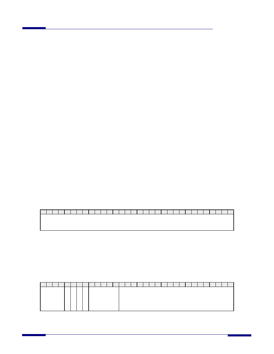
System Software Data Register
Address Offset: 4CH / 24CH
Access Type: Read/Write
Reset Value: Undefined
31 30 29 28 27 26 25 24 23 22 21 20 19 18 17 16 15 14 13 12 11 10 09 08 07 06 05 04 03 02 01 00
System Software Data
This register is used by the software for non-resettable data storage. The contents are unknown on power-up and
are never cleared by any type of reset.
Flash Memory Address – Command + Status
Address Offset: 50H
Access Type: Read/Write
Reset Value: 0x0800_0000
31 30 29 28 27 26 25 24 23 22 21 20 19 18 17 16 15 14 13 12 11 10 09 08 07 06 05 04 03 02 01 00
Reserved
M
e
m
Init
Done
M
e
m
Init
M
e
m
A
c
cess
St
art
M
e
m
A
ccess
Type
Reserved
Memory Address
This register defines the address and command/status register for flash memory interface in the SiI3114. The
register bits are defined below.
相關(guān)PDF資料 |
PDF描述 |
|---|---|
| SII3114CTU | PCI BUS CONTROLLER, PQFP176 |
| SII3124ACBHU | PCI BUS CONTROLLER, PBGA364 |
| SII3512ECTU128 | PCI BUS CONTROLLER, PQFP128 |
| SII3531ACNU | PCI BUS CONTROLLER, QCC48 |
| SIO10N268-NU | MULTIFUNCTION PERIPHERAL, PQFP128 |
相關(guān)代理商/技術(shù)參數(shù) |
參數(shù)描述 |
|---|---|
| SII3114CTU | 制造商:Silicon Image Inc 功能描述:PCI to Serial ATA Controller 176-Pin TQFP 制造商:SILICON 功能描述: |
| SII3124A | 制造商:SILICONIMAGE 制造商全稱:SILICONIMAGE 功能描述:PCI-X to Serial ATA Controller |
| SII3124ACBHU | 制造商:SILICONIMAGE 制造商全稱:SILICONIMAGE 功能描述:PCI-X to Serial ATA Controller |
| SII3132 | 制造商:SILICONIMAGE 制造商全稱:SILICONIMAGE 功能描述:PCI Express to 2-Port Serial ATA II Host Controller |
| SII3132CNU | 制造商:Silicon Image Inc 功能描述:PCI Express to Serial ATA Controller 88-Pin QFN |
發(fā)布緊急采購,3分鐘左右您將得到回復(fù)。